Showing posts with label circuit. Show all posts
Showing posts with label circuit. Show all posts
Thursday, November 10, 2016
Simple Peak Detector Circuit
Simple Peak Detector Circuit
In this article we are going to learn about a peak detector circuit, its working principle and how to implement it in clap operated circuits for illuminating an LED in response to clap sounds.
By: Girish Radhakrishnan
A peak detector is a circuit which holds maximum amplitude value of a signal. If a signal varies rapidly and we are unable to measure it, then we go for peak detector. This circuit holds the maximum amplitude value for short period of time so that we can measure it.
There are many ways to do this and often used in many fields in electronics where rapid measurement is not viable.
For instance, taking heat gun thermometer as example, where the temperature of an object may vary rapidly at some situations, the peak value of temperature and current value of temperature is displayed simultaneously so that user can get an idea about the object.
Similarly, there are many situations in electronics, where we may need to measure peak signals.
Here, we are going to see simple peak detector circuit that consists of one diode, one capacitor and one resistor.
The diode permits the current in one direction, which is to charge the capacitor.
When the input drops the capacitor holds the value for a short period which gives some time to measure the peak. Here the short period could be ranging from a few milliseconds to a few seconds.
The values need to be refreshed time to time so that new values can be stored. To do this we need to discharge the capacitor. A bleed resistor is connected parallel to capacitor which discharges.

The capacitor discharge time can be calculated by the following formula:
T = 5 x C x R
Where, T is time in seconds
C is capacitance in Farad
R is resistance in Ohm
Clap Sensor circuit:
Here, we will implement the peak detector in a clap sensor circuit. This circuit responds to loud busts of sound such as clap.
There are three stages in this circuit, the microphone amplifier, peak detector and op-amp circuit that detects peak.
The sound gets converted to electrical signal by the microphone, gets amplified by op-amp. The amplified signal enters the peak detector circuit and charges the capacitor. The peak value stored in the capacitor becomes the peak input minus 0.7V for silicon diodes, since there will be always voltage drop across diode.

The value stored in the capacitor gets recognized by op-amp comparator circuit.
As soon as the peak value goes above reference voltage the LED turns ON.
As soon as the capacitor is discharged below reference voltage the LED turns OFF.
So, what was the role of peak detector in this circuit? Well, it holds the clap signal for few 100 milliseconds which helped the LED to stay illuminated for a few 100 milliseconds. If you wish LED to light longer, it can be done by incrementing capacitance and resistor values.
By: Girish Radhakrishnan
What is peak detector?
A peak detector is a circuit which holds maximum amplitude value of a signal. If a signal varies rapidly and we are unable to measure it, then we go for peak detector. This circuit holds the maximum amplitude value for short period of time so that we can measure it.
There are many ways to do this and often used in many fields in electronics where rapid measurement is not viable.
For instance, taking heat gun thermometer as example, where the temperature of an object may vary rapidly at some situations, the peak value of temperature and current value of temperature is displayed simultaneously so that user can get an idea about the object.
Similarly, there are many situations in electronics, where we may need to measure peak signals.
How it works?
Here, we are going to see simple peak detector circuit that consists of one diode, one capacitor and one resistor.
The diode permits the current in one direction, which is to charge the capacitor.
When the input drops the capacitor holds the value for a short period which gives some time to measure the peak. Here the short period could be ranging from a few milliseconds to a few seconds.
The values need to be refreshed time to time so that new values can be stored. To do this we need to discharge the capacitor. A bleed resistor is connected parallel to capacitor which discharges.
The capacitor discharge time can be calculated by the following formula:
T = 5 x C x R
Where, T is time in seconds
C is capacitance in Farad
R is resistance in Ohm
Clap Sensor circuit:
Here, we will implement the peak detector in a clap sensor circuit. This circuit responds to loud busts of sound such as clap.
There are three stages in this circuit, the microphone amplifier, peak detector and op-amp circuit that detects peak.
The sound gets converted to electrical signal by the microphone, gets amplified by op-amp. The amplified signal enters the peak detector circuit and charges the capacitor. The peak value stored in the capacitor becomes the peak input minus 0.7V for silicon diodes, since there will be always voltage drop across diode.
The value stored in the capacitor gets recognized by op-amp comparator circuit.
As soon as the peak value goes above reference voltage the LED turns ON.
As soon as the capacitor is discharged below reference voltage the LED turns OFF.
So, what was the role of peak detector in this circuit? Well, it holds the clap signal for few 100 milliseconds which helped the LED to stay illuminated for a few 100 milliseconds. If you wish LED to light longer, it can be done by incrementing capacitance and resistor values.
Available link for download

Tuesday, November 8, 2016
Synchronized 4kva Stackable Inverter Circuit Part 2
Synchronized 4kva Stackable Inverter Circuit Part 2
In the previous part of this article we learned the main section of the 4kva synchronized stackable inverter circuit which explained the synchronization details of the design. In this article we study how to make the design a sinewave equivalent and also ensure correct synchronization of the PWMs across the involved inverters.
Synchronizing Sine Wave PWM across the Inverters
A simple RMS matched PWM equivalent sinewave waveform generator can be made by using an IC 555 and IC 4060, as shown in the following figure.This design can be then used for enabling the inverters to produce a sinewave equivalent waveform at their outputs, and across the connected mains line.
Each of these PWM processors would be required for each of the stackable inverter modules individually.

The different stages involved in the above PWM geneartor circuit can be understood with the help of the following point:
The IC 555 is configured as the basic PWM generator circuit. To be able to generate an adjustable PWM equivalent pulses at the desired RMS the IC requires fast triangle waves at its pin7 and a reference potential at its pin5 which determines the PWM level at its output pin#3
For generating the triangle waves, the IC 555 requires square waves at its pin#2, which is acquired from the IC 4060 oscillator chip.
The IC 4060 determines the frequency of the PWM, or simply the number of "pillars" in each of the AC half cycles.
The IC 4060 is mainly employed for multiplying the sample low frequency content from the inverter output into a relatively high frequency from its pin#7. The sample frequency basically makes sure that the PWM chopping is equal and synchronized for all the invetrer modules. This is main reason why the IC 4060 is included otherwise another IC 555 could have easy done the job, instead.
The reference potential at pin#5 of IC 555 is acquired from an opamp voltage follower shown at extreme left of the circuit.
As the name suggests this opamp delivers exactly the same magnitude of voltage at its pin#6 which appears at its pin#3....however the pin#6 replication of its pin#3 is nicely buffered, and therefore is richer than its pin3 quality, and thats the exact reason of including this stage in the design.
The 10 k preset associated at pin3 of this IC is used for adjusting the RMS level which ultimately fine tunes the the IC 555 output PWMs to the desired RMS level.
This RMS is then applied to the bases of the power devices in order to force them to work at the specified PWM RMS levels, which in turn causes the output AC to acquire a pure sinewave like attribute through a correct RMS level. This may be further enhanced by employing an LC filter across the output winding of the all the transformers.
The next and the final part of this 4kva stackable synchronized inverter circuit details the automatic load correction feature for enabling the inverters to deliver and maintain the correct amount wattage across the output power mains line in accordance with the varying loads switching.
Available link for download
Saturday, November 5, 2016
Motorcycle Shunt Regulator Circuit using SCR
Motorcycle Shunt Regulator Circuit using SCR
The circuit presented here is a Rectifier plus Regulator for a 3-Phase charging system of Motorcycles. The rectifier is full-wave and the regulator is shunt-type regulator.
By: Abu Hafss
A motorcycles charging system is different from that on cars. The voltage alternator or generator on cars are electro-magnet type which are quite easy to regulate. Whereas, the generators on motorcycles are permanent magnet type. The voltage output of an alternator is directly proportional to the RPM i.e. at high RPM the alternator will produce high voltages more than 50V hence, a regulator becomes essential to protect the entire electrical system and the battery too.
Some small bikes and 3-wheelers which do not run at high speeds, only have 6 diodes (D6-D11) to perform full-wave rectification. They dont need regulation but those diodes are high ampere rated and dissipate a lot of heat during operation.
In bikes with proper regulated charging systems, normally shunt-type regulation is used. This is done by shorting out the alternators windings for one cycle of the AC waveform. An SCR or sometimes a transistor is used as shunting device in each phase.

For the rectifier, there are three options:
a) Six automotive diodes
b) One 3-phase rectifier
c) Two bridge rectifiers
All must be rated at least 15A and heat-sinked.
The automotive diodes are two types positive body or negative body hence, should be used accordingly. But they might be little difficult to contact to heat-sink.
If using two bridge rectifiers, they may be used as shown.
By: Abu Hafss
A motorcycles charging system is different from that on cars. The voltage alternator or generator on cars are electro-magnet type which are quite easy to regulate. Whereas, the generators on motorcycles are permanent magnet type. The voltage output of an alternator is directly proportional to the RPM i.e. at high RPM the alternator will produce high voltages more than 50V hence, a regulator becomes essential to protect the entire electrical system and the battery too.
Some small bikes and 3-wheelers which do not run at high speeds, only have 6 diodes (D6-D11) to perform full-wave rectification. They dont need regulation but those diodes are high ampere rated and dissipate a lot of heat during operation.
In bikes with proper regulated charging systems, normally shunt-type regulation is used. This is done by shorting out the alternators windings for one cycle of the AC waveform. An SCR or sometimes a transistor is used as shunting device in each phase.
The network C1, R1, R2, ZD1, D1 and D2 forms the voltage detection circuit, and it is designed to trigger at about 14.4 volts. As soon as charging system passes this threshold voltage, T1 starts conducting. This sends current to each gate of the three SCRs S1, S2 and S3, via current limiting resistors R3, R5 and R7. D3, D4 and D5 are important to isolate the gates from each other. R4, R6 and R8 help in draining any possible leakage from T1. S1, S2 & S3 should be heat-sinked and isolated from each other using mica insulator, if using common heat-sink.
For the rectifier, there are three options:
a) Six automotive diodes
b) One 3-phase rectifier
c) Two bridge rectifiers
All must be rated at least 15A and heat-sinked.
The automotive diodes are two types positive body or negative body hence, should be used accordingly. But they might be little difficult to contact to heat-sink.
If using two bridge rectifiers, they may be used as shown.
  |
| Bridge Rectifier |
 |
| Automotive diodes |
 |
| 3-phase rectifier |
 |
| Bridge Rectifier |
Available link for download
Friday, November 4, 2016
Synchronized 4kva Stackable Inverter Circuit Part 3
Synchronized 4kva Stackable Inverter Circuit Part 3
We have so far covered the two main requirements for the proposed synchronized 4kva stackable inverter circuit, which includes synchronization of frequency, phase and PWM across the inverters so that failing of any of the inverters had no effect on the rest in terms of the above parameters.
In this article we will try to figure out the automatic load correction feature which may enable the switching ON or OFF of the inverters sequentially in response to the varying load conditions across the output mains line.
A simple quad comparator using LM324 IC can be used for implementing an automatic sequential load correction as indicated in the following diagram:

In the figure above we can see four opamps from the IC LM324 configured as four separate comparators with their non-inverting inputs rigged with individual presets,while their inverting inputs all referenced with a fixed zener voltage.
The relevant presets are simply adjusted such that the opamps produce high outputs in a sequential a soon as the mains voltage goes above the intended threshold..... and vice versa.
When this happens the relevant transistors switch in accordance with the opamp activation.
The collectors of the respective BJTs are connected with the pin#3 of the voltage follower opamp IC 741 which is employed in the PWM controller stage, and this forces the opamp output to go low or zero, which in turn causes a zero voltage to appear at pin#5 of the PWM IC 555 (as discussed in Part 2).
With pin#5 of the IC 555 is applied with this zero logic, forces the PWMs to become narrowest or at the minimum value, which causes the output of that particular inverter to almost shut down.
The above actions make an attempt to stabilize the output to an earlier normal condition which again forces the PWM to get wider and this tug-of-war or a constant switching of the opamps cintinues consistently keeping the output as stable as possible, in response to the variations of the attached loads.
With this automatic load correction implemented within the proposed 4kva stackable inverter circuit almost makes the design complete with all the features requested by the user in Part 1 of the article.
In this article we will try to figure out the automatic load correction feature which may enable the switching ON or OFF of the inverters sequentially in response to the varying load conditions across the output mains line.
A simple quad comparator using LM324 IC can be used for implementing an automatic sequential load correction as indicated in the following diagram:
In the figure above we can see four opamps from the IC LM324 configured as four separate comparators with their non-inverting inputs rigged with individual presets,while their inverting inputs all referenced with a fixed zener voltage.
The relevant presets are simply adjusted such that the opamps produce high outputs in a sequential a soon as the mains voltage goes above the intended threshold..... and vice versa.
When this happens the relevant transistors switch in accordance with the opamp activation.
The collectors of the respective BJTs are connected with the pin#3 of the voltage follower opamp IC 741 which is employed in the PWM controller stage, and this forces the opamp output to go low or zero, which in turn causes a zero voltage to appear at pin#5 of the PWM IC 555 (as discussed in Part 2).
With pin#5 of the IC 555 is applied with this zero logic, forces the PWMs to become narrowest or at the minimum value, which causes the output of that particular inverter to almost shut down.
The above actions make an attempt to stabilize the output to an earlier normal condition which again forces the PWM to get wider and this tug-of-war or a constant switching of the opamps cintinues consistently keeping the output as stable as possible, in response to the variations of the attached loads.
With this automatic load correction implemented within the proposed 4kva stackable inverter circuit almost makes the design complete with all the features requested by the user in Part 1 of the article.
Available link for download
Thursday, November 3, 2016
Simple Vertical Axis Wind Turbine Generator Circuit
Simple Vertical Axis Wind Turbine Generator Circuit
The post explains a simple vertical axis wind turbine generator circuit using ready made high power generator dynamo and a vertical axis wind turbine mechanism. The idea was requested by Mr. Taibani.
The Request
Hello Swagatam,
Bro hope youre doing well.
Firstly thanks for all the great knowledge & information you have given here its really appreciated.
I am trying to do a project of home made low RPM VAWT generator which can generate enough power to run one small scale factory I need your help on winding section.
1) Correct copper winding design for low rpm.
2) Correct copper wire gauge.
3) Number of turns of winding.
4) What core material should be used for low drag ( Lenz effect ).
Please help me out & your readers with your great knowledge.
Thanks & Regards,
Taibani Imran.
The Design
Designing a VAWT motor is not easy and might require good expertise in the field and at the moment for me this looks much complex and I have little idea regarding the same.
However for any layman the idea could be easily implemented through a ready made generator as described below:
Below is an example of a 10,000 watt dynamo which could be used for the proposed vertical axis wind turbine generator application

Instead of winding a vertical axis wind generator yourself, a simpler idea would be to configure the VAWT mechanism with a high watt generator or a dynamo through a correctly calculated gear or pulley/belt ratio.
For example, the above shown 10 kv dynamo has a specifications of generating 10000 watt at around 3600 RPM, which implies that if the a pulley ratio of 1:100 is configured, the dynamo would be able to produce the rated amount of power with the VAWT rotating at just around 36 RPM, which could be achieved perhaps even at wind speeds as low as 5km per hour.
The following diagram shows a rough set up design for the above explained implementation:

The figure above shows a simple vertical axis wind turbine model, the vertical helical turbine is designed to capture wind flow on one half of its span while allow free flow on the other half, causing the propeller to initiate a rotational movement with high torque.
Being vertical in its positioning the VAWT does not rely on wind directions unlike the traditional horizontal axis wind turbines. This advantage makes the VAWT sustain its operations under all wind conditions regardless of its direction of flow.
The central vertical axis of the turbine can be seen attached with a gigantic flywheel, which is supposed to be a lot bigger than the wheel attached with the generator shaft.
The bigger the ratio, the bigger would be the conversion even at minimal wind speeds.
With a ratio of 1:100, the generator could be expected to be generating at its full capacity and specification, with the VAWT moving at a meager 50 RPM or even less. This speed could be in turn achieved at wind speeds not exceeding 5 to 10 miles per hour.
The above explained set up is for facilitating efficient conversions at low wind speeds, but what happens when the wind is rapid or during stormy conditions.
If this situation is not taken care of can easy rip-of the generator winding and burn it within no time.
In order to control the VAWT speed at dangerous wind speeds, the following shunt regulator circuit could be used with the output of the generator for achieving a constant speed on the generator and the VAWT.

In the above figure the generator output is applied to a high current triac shunt regulator network through a 50 amp bridge rectifier module.
The value of the zener diode determines the control threshold, which is shown as 220V in the diagram. It means under no circumstances the voltage from the generator can exceed the 220V mark, and if it does the excess power is simply shunted or shorted to ground via the triac.
This ensures a controlled rotation of the generator even at formidable wind speeds keeping the entire system stabilized and safe.
If the generator used is a 3 phase type of generator, the shunt regulator shown above could be replaced with a 3 phase shunt regulator using SCRs.
If you have any doubts regarding the discussed vertical axis wind turbine generator circuit, do feel free to express them through comments
The Request
Hello Swagatam,
Bro hope youre doing well.
Firstly thanks for all the great knowledge & information you have given here its really appreciated.
I am trying to do a project of home made low RPM VAWT generator which can generate enough power to run one small scale factory I need your help on winding section.
1) Correct copper winding design for low rpm.
2) Correct copper wire gauge.
3) Number of turns of winding.
4) What core material should be used for low drag ( Lenz effect ).
Please help me out & your readers with your great knowledge.
Thanks & Regards,
Taibani Imran.
The Design
Designing a VAWT motor is not easy and might require good expertise in the field and at the moment for me this looks much complex and I have little idea regarding the same.
However for any layman the idea could be easily implemented through a ready made generator as described below:
Below is an example of a 10,000 watt dynamo which could be used for the proposed vertical axis wind turbine generator application
Instead of winding a vertical axis wind generator yourself, a simpler idea would be to configure the VAWT mechanism with a high watt generator or a dynamo through a correctly calculated gear or pulley/belt ratio.
For example, the above shown 10 kv dynamo has a specifications of generating 10000 watt at around 3600 RPM, which implies that if the a pulley ratio of 1:100 is configured, the dynamo would be able to produce the rated amount of power with the VAWT rotating at just around 36 RPM, which could be achieved perhaps even at wind speeds as low as 5km per hour.
The following diagram shows a rough set up design for the above explained implementation:
The figure above shows a simple vertical axis wind turbine model, the vertical helical turbine is designed to capture wind flow on one half of its span while allow free flow on the other half, causing the propeller to initiate a rotational movement with high torque.
Being vertical in its positioning the VAWT does not rely on wind directions unlike the traditional horizontal axis wind turbines. This advantage makes the VAWT sustain its operations under all wind conditions regardless of its direction of flow.
The central vertical axis of the turbine can be seen attached with a gigantic flywheel, which is supposed to be a lot bigger than the wheel attached with the generator shaft.
The bigger the ratio, the bigger would be the conversion even at minimal wind speeds.
With a ratio of 1:100, the generator could be expected to be generating at its full capacity and specification, with the VAWT moving at a meager 50 RPM or even less. This speed could be in turn achieved at wind speeds not exceeding 5 to 10 miles per hour.
Controlling VAWT speed using Shunt Regulator Circuit
The above explained set up is for facilitating efficient conversions at low wind speeds, but what happens when the wind is rapid or during stormy conditions.
If this situation is not taken care of can easy rip-of the generator winding and burn it within no time.
In order to control the VAWT speed at dangerous wind speeds, the following shunt regulator circuit could be used with the output of the generator for achieving a constant speed on the generator and the VAWT.
In the above figure the generator output is applied to a high current triac shunt regulator network through a 50 amp bridge rectifier module.
The value of the zener diode determines the control threshold, which is shown as 220V in the diagram. It means under no circumstances the voltage from the generator can exceed the 220V mark, and if it does the excess power is simply shunted or shorted to ground via the triac.
This ensures a controlled rotation of the generator even at formidable wind speeds keeping the entire system stabilized and safe.
If the generator used is a 3 phase type of generator, the shunt regulator shown above could be replaced with a 3 phase shunt regulator using SCRs.
If you have any doubts regarding the discussed vertical axis wind turbine generator circuit, do feel free to express them through comments
Available link for download
Wednesday, November 2, 2016
Remote Control Circuit Using Arduino
Remote Control Circuit Using Arduino
In this post, we are going to construct a remote control circuit for controlling home appliances using arduino microcontroller.
By: Girish Radhakrishnan
This circuit can turn on/off your gadgets using TV remote’s unused buttons or any other unused remote that may be lying in your junk box for ages.
The motto of this project is to help physically challenged persons, and help them to access the ON/OFF switching of the basic home appliances such as fans or lights independently.
The second objective is to enable the user to control the gadgets “Like a boss” without having to move from his or her existing position.
The circuit utilizes traditional IR based communication between transmitter and receiver.
This circuit is cent percent fool proof to other IR remotes, and other IR sources and less susceptible to errors.
The major problem with non-microcontroller based IR remote control circuit, which is found around the internet, is that it could turn ON/OFF with any IR based remote and can only control one device at an instant and also more susceptible to errors.
This circuit overcomes above specified issues, and we can control several gadgets on one remote and assign keys for specific gadgets.
Before proceeding this project you need to download the library files for arduino form this link and follow the instruction given below: https://github.com/z3t0/Arduino-IRremote
Instructions:
1) Click “clone or download” button form the given link and hit “Download ZIP”.
2) Extract the file and move “IRremote” folder to your library folder of Arduino.
3) Delete “RobotIRremote” folder from your arduino library. “RobotIRremote” has similar definition of “IRremote” library which clash and not able to upload the code to Arduino so, deletion/removal is mandatory.
By duplicating the above instruction your Arduino IDE software is ready for any/most of the IR based projects.
Assign keys for remote:
In our TV remote each key has unique hexadecimal code, which is used to recognize which key is pressed for an operation. Before uploading the final code to Arduino, you need to find what the hexadecimal codes for your keys are.
To do this construct the following circuit in breadboard and follow the instruction.
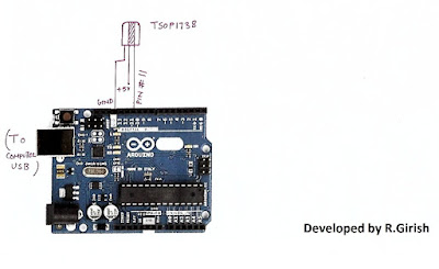
1) Open Arduino IDE and upload example code “IRrecv Demo”
2) Open serial monitor and press the key on remote that you want to use.
You’ll see hexadecimal code pop up as soon as you press the key. That’s the hexadecimal code for that particular key.
3) Do the same for other two keys (3 keys are given in this project for controlling 3 devices)
· We are going to use these hexadecimal codes in the main program and upload to arduino.
//-----------------Program developed by R.Girish-----------//
#include<IRremote.h>
int input = 11;
int op1 = 8;
int op2 = 9;
int op3 = 10;
int intitial1;
int intitial2;
int intitial3;
IRrecv irrecv(input);
decode_results dec;
#define output1 0x111 // place your code received from button A
#define output2 0x112 // place your code received from button B
#define output3 0x113 // place your code received from button C
void setup()
{
irrecv.enableIRIn();
pinMode(op1,1);
pinMode(op2,1);
pinMode(op3,1);
}
void loop() {
if (irrecv.decode(&dec)) {
unsigned int value = dec.value;
switch(value) {
case output1:
if(intitial1 == 1) {
digitalWrite(op1, LOW);
intitial1 = 0;
} else {
digitalWrite(op1, HIGH);
intitial1 = 1;
}
break;
case output2:
if(intitial2 == 1) {
digitalWrite(op2, LOW);
intitial2 = 0;
} else {
digitalWrite(op2, HIGH);
intitial2 = 1;
}
break;
case output3:
if(intitial3 == 1) {
digitalWrite(op3, LOW);
intitial3 = 0;
} else {
digitalWrite(op3, HIGH);
intitial3 = 1;
}
break;
}
irrecv.resume();
}
}
//--------------Program developed by R.Girish-----------//
NOTE:
In the program:
#define output1 0x111 // place your code received from button A
#define output2 0x111 // place your code received from button B
#define output3 0x111 // place your code received from button C
· Place your 3 unique codes from your remote in this place of 111, 112, and 113 and upload the code. Hexadecimal codes will be from 0 to 9 and A to F, for example: 20156, 26FE789, FFFFFF.
· Place your code with “0x” (zero x).
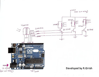
Circuit diagram:
· Pressing key trips the relay ON and by pressing again it will turn off the relay.
Available link for download
Simple Refrigerator Protector Circuit
Simple Refrigerator Protector Circuit
This simple refrigerator protector circuit is actually a delay ON timer circuit which makes sure that whenever a power failure occurs or in case abrupt power fluctuations take place, the refrigerator is never allowed to switch ON instantly, rather after a delay of a few moments.
Today most modern refrigerators are equipped with a protection feature which prevents the fridge from suddenly switching ON or OFF due to sudden power fluctuations or a sudden power restoration.
However, for those fridges which are not equipped with this feature, the following simple delay ON timer circuit can be applied to enable the refrigerator to switch ON after a certain delay, and only when the mains power has become stable. Until this happens the circuit keeps the fridge switched OFF and monitors until the power has returned to a perfectly normal status.
Referring to the above shown refrigerator protection circuit, we are able to witness a two transistor circuit which forms a very basic yet effective delay ON timer circuit, meaning this circuit switches ON its output after some delay, after power is applied to it.
The power supply to the circuit is derived from the mains via a transformerless power supply circuit
which is appropriately stabilized at 12V and fed to the delay circuit.
Whenever power is switched ON, may it be during the first initialization, or during a power failure situation, the associated 1000uF capacitor prevents the BC547 from switching ON at the onset, which in turn keeps the BC557 and the triac switched OFF. The load is therefore unable to receive power and stays switched OFF too.
However, the 1000uF now gradually begins charging via the 330K resistor and when the potential difference across it reaches the approximate total of transistors biasing limit plus the emitter zener value (0.6 + 3 = 3.6V), the transistor begins switching ON which prompts the BC557 also to switch ON.
The triac now begins acquiring the required gate voltage and within moments switches ON the fridge.
The 1000uF capacitor stays charged as long as power is available to the circuit, and during power failures the capacitor discharges through the parallel 100k resistor so that it can get into the standby mode for the next delay ON cycle operation.
The time delay period can be accomplished by appropriately selecting the values of the 330K resistor, the 1000uF capacitor and the 3V zener diode, as per the users preference.
This concludes the explanation for the proposed simple refrigerator protection circuit, for any related query please feel free to use the comment box.
Today most modern refrigerators are equipped with a protection feature which prevents the fridge from suddenly switching ON or OFF due to sudden power fluctuations or a sudden power restoration.
However, for those fridges which are not equipped with this feature, the following simple delay ON timer circuit can be applied to enable the refrigerator to switch ON after a certain delay, and only when the mains power has become stable. Until this happens the circuit keeps the fridge switched OFF and monitors until the power has returned to a perfectly normal status.
 |
| WARNING: CIRCUIT IS NOT ISOLATED FROM MAINS... STRICT PRECAUTIONS MUST BE OBSERVED WHILE HANDLING THE DEVICE, WHILE ITS IN AN UNENCLOSED CONDITION. |
Referring to the above shown refrigerator protection circuit, we are able to witness a two transistor circuit which forms a very basic yet effective delay ON timer circuit, meaning this circuit switches ON its output after some delay, after power is applied to it.
The power supply to the circuit is derived from the mains via a transformerless power supply circuit
which is appropriately stabilized at 12V and fed to the delay circuit.
Whenever power is switched ON, may it be during the first initialization, or during a power failure situation, the associated 1000uF capacitor prevents the BC547 from switching ON at the onset, which in turn keeps the BC557 and the triac switched OFF. The load is therefore unable to receive power and stays switched OFF too.
However, the 1000uF now gradually begins charging via the 330K resistor and when the potential difference across it reaches the approximate total of transistors biasing limit plus the emitter zener value (0.6 + 3 = 3.6V), the transistor begins switching ON which prompts the BC557 also to switch ON.
The triac now begins acquiring the required gate voltage and within moments switches ON the fridge.
The 1000uF capacitor stays charged as long as power is available to the circuit, and during power failures the capacitor discharges through the parallel 100k resistor so that it can get into the standby mode for the next delay ON cycle operation.
The time delay period can be accomplished by appropriately selecting the values of the 330K resistor, the 1000uF capacitor and the 3V zener diode, as per the users preference.
This concludes the explanation for the proposed simple refrigerator protection circuit, for any related query please feel free to use the comment box.
Available link for download
Sunday, October 30, 2016
Small Induction Heater Circuit for School Project
Small Induction Heater Circuit for School Project
The post discusses a small induction heater circuit for school project and exhibitions, using a very ordinary IC 555 astable PWM circuit. The idea was requested by Mr. Anthony
The Request
Hi,
for a school project i need to construct an AC induction cooktop and was wondering if you could help me put together a part list for a much weaker induction cooktop than yours, it only has to warm up a few MLs of water. is this something that is possible?
The Design
An induction heater is considered as an amazing circuit which is capable of converting electricity into heat with utmost efficiency and without much losses.
However a little contemplation will make you realize that actually its just the opposite. An induction heater circuit is an extremely inefficient circuit which converts all the electricity into heat.
This opinion is with regards to the general view about electrical and electronic circuits where the emission of heat is considered to be inefficient and undesirable.
But for an induction heater, this inefficiency attribute becomes its positive aspect, and the more inefficiently it is designed, the more beneficial it becomes for the user.
To be precise, an induction heater is an inefficient transformer which is purposely mismatched with its frequency and the core material specifications.
In this concept the core is normally a ferromagnetic material such as iron having a copper coil wound over it. The copper winding around this iron core is oscillated at a relatively higher frequency which may be not suited for the iron material.
The bad conductor nature of iron finds it difficult to resonate at the high winding frequency resulting in the generation of high back emf eddy currents which in turn causes high temperatures on the core material.
This feature is exploited in induction heaters for the intended purpose of achieving high temperatures
Although massive induction heater units can be built for generating extremely high temperatures using the same concept, a small induction heater circuit for school exhibition project can also be implemented easily using ordinary parts such as a IC 555 and some other inexpensive passive components.

A simple IC 555 induction heater circuit for school project is shown in the above figure.
Here the IC is configured as a PWM generator circuit, which is adjusted using the 5 K pot. The frequency is adjusted by tweaking the 1M pot or the 1uF capacitor specifically for achieving the optimized heating effect on the work coil.
The working coil here is made by winding around 50 turns (not critical) of 1mm super enameled copper wire over a fabricated iron pipe whose dimensions may be selected as per individual preference, and could be anywhere between 10 to 20 cm in diameter and 30 to 40 cms long.
Once the above set up is built and switched ON, the coil and the iron pipe could be seen developing heat gradually, and anything placed inside the pipe could be witnessed getting heated up.
If its water inside the pipe, then it could begin warming up and even reach the boiling point if the coil is optimized correctly through the frequency and PWM adjustments.
The idea behind this small induction heater circuit is simple, it is to force the iron pipe atoms to electromagnetically oscillate at an incompatible frequency resulting in the production of huge amounts of opposing eddy currents and a proportionate amount of heat due to this opposing current in the metal.
If you have more questions regarding this induction heater circuit for school science project, do feel free to ask them through comments, below.
The Request
Hi,
for a school project i need to construct an AC induction cooktop and was wondering if you could help me put together a part list for a much weaker induction cooktop than yours, it only has to warm up a few MLs of water. is this something that is possible?
The Design
An induction heater is considered as an amazing circuit which is capable of converting electricity into heat with utmost efficiency and without much losses.
However a little contemplation will make you realize that actually its just the opposite. An induction heater circuit is an extremely inefficient circuit which converts all the electricity into heat.
This opinion is with regards to the general view about electrical and electronic circuits where the emission of heat is considered to be inefficient and undesirable.
But for an induction heater, this inefficiency attribute becomes its positive aspect, and the more inefficiently it is designed, the more beneficial it becomes for the user.
To be precise, an induction heater is an inefficient transformer which is purposely mismatched with its frequency and the core material specifications.
In this concept the core is normally a ferromagnetic material such as iron having a copper coil wound over it. The copper winding around this iron core is oscillated at a relatively higher frequency which may be not suited for the iron material.
The bad conductor nature of iron finds it difficult to resonate at the high winding frequency resulting in the generation of high back emf eddy currents which in turn causes high temperatures on the core material.
This feature is exploited in induction heaters for the intended purpose of achieving high temperatures
Although massive induction heater units can be built for generating extremely high temperatures using the same concept, a small induction heater circuit for school exhibition project can also be implemented easily using ordinary parts such as a IC 555 and some other inexpensive passive components.
A simple IC 555 induction heater circuit for school project is shown in the above figure.
Here the IC is configured as a PWM generator circuit, which is adjusted using the 5 K pot. The frequency is adjusted by tweaking the 1M pot or the 1uF capacitor specifically for achieving the optimized heating effect on the work coil.
The working coil here is made by winding around 50 turns (not critical) of 1mm super enameled copper wire over a fabricated iron pipe whose dimensions may be selected as per individual preference, and could be anywhere between 10 to 20 cm in diameter and 30 to 40 cms long.
Once the above set up is built and switched ON, the coil and the iron pipe could be seen developing heat gradually, and anything placed inside the pipe could be witnessed getting heated up.
If its water inside the pipe, then it could begin warming up and even reach the boiling point if the coil is optimized correctly through the frequency and PWM adjustments.
The idea behind this small induction heater circuit is simple, it is to force the iron pipe atoms to electromagnetically oscillate at an incompatible frequency resulting in the production of huge amounts of opposing eddy currents and a proportionate amount of heat due to this opposing current in the metal.
If you have more questions regarding this induction heater circuit for school science project, do feel free to ask them through comments, below.
Available link for download
Thursday, October 27, 2016
Sinewave UPS Circuit using PIC16F72 Part 5
Sinewave UPS Circuit using PIC16F72 Part 5
In this write-up we try to understand in detail regarding the various possible faults that could be encountered while constructing the proposed sinewave UPS circuit using PIC16F72. and how to troubleshoot these issues effectively through simple steps.
Data provided by: Mr. hisham bahaa-aldeen (hisham2630@gmail.com)
Sinewave UPS Circuit using PIC16F72 Part-1
Sinewave UPS Circuit using PIC16F72 Part-2
Sinewave UPS Circuit using PIC16F72 Part-3
Sinewave UPS Circuit using PIC16F72 Part-4

Construct the card thereby confirming each and every wiring, this includes LED connectivity, ON/OFF switch, feedback via inverter transformer, 6-volt mains sense to CN5, -VE of battery to card, +VE of battery to large heatsink.
Initially do not plug the transformer primary to the pair of small heat sinks.
Plug in battery +ve wire to PCB via MCB and 50-amp ammeter.
Prior to proceeding for the recommended testings be sure to check the +VCC voltage at the pins of U1 - U5 in the following sequence.
U1:pin#8 and 9: +5V, pin#3: +12V, pin#6: +12V, U2:pin#8 and 9: +5V, pin#3: +12V, pin6: +12V, U3: pin14: +5V, U4: pin20: +5V, pin1:+5V, U5: pin4:+5V.
1) Power Up the battery MCB and check the ammeter and also be certain it doesnt jump beyond 1-amp. If the ampere shoots then remove U1 and U2 briefly and switch ON the MCB again.
2) Power ON by toggling the given ON/OFF switch of the inverter and check whether or not the relay clicks ON, illuminating the "INV" LED. If it doesnt then check the voltage at pin#18 of the PIC which is supposed to be 5V. If this is absent check components R37 and Q5, one of this may be faulty or incorrectly connected. If you find the "INV" LED not switching ON, check if the voltage at pin#25 of the PIC is 5V or not.
If the above situation is seen to be normally executing, go to the next step as described below.
3) Using an oscilloscope test pin#13 of the PIC by alternately switching ON/OFF the inverter switch, you can expect to see a well modulated PWM signal appearing at this pinout each time the inverter mains input is switched OFF, if not then you can assume the PIC to be faulty, coding not implemented correctly or the IC is badly soldered or inserted in its socket.
If you succeed in getting the expected modified PWM feed over this pin, go to pin#12/in#14 of the IC and check the availability of 50Hz frequency on these pins, if not would indicate some fault in the PIC configuration, remove and replace it. If you are to get affirmative response on these pins, go to the next step as explained below.
4) The next step would be to test pin#10/pin#12 of the IC U3 (CD4081) for the modulated PWMs which are finally integrated with the mosfet driver stages U1 and U2. Additionally you would be also required to check the potential differences at pin#9/pin#12 which is supposed to be at 3.4V approximately, and at pin#8/pin#13 may be verified to be at 2.5V. Similarly verify pin#10/11 to be at 1.68V.
In case you fail to identify the modulated PWM across the CD4081 output pins, then you would want to verify the tracks terminating to the relevant pins of the IC CD4081 from the PIC, which could be broken or somehow the obstructing the PWMs from the reaching U3.
If all is fine, lets move to the next level.
5) Next, attach the CRO with U1 gate, toggle the inverter ON/OFF and as done above verify the PWMs on this spot which are M1 and M4, and also the gates M9, M12, however dont be surprised if the PWM switching are seen out of phase M9/M12 as compared to M1/M4, thats normal.
If the PWMs are entirely absent on these gates, then you can check pin#11 of U1 which is expected to be low, and if found high would indicate that U1 may be running in the shut-down mode. To confirm this situation check voltage at pin#2 of U5 which could be at 2.5V, and identically pin#3 of U5 could be at 0V or under 1V, if its detected to be below 1V, then proceed and check R47/R48, but if the voltage is found to be above 2.5V then check D11, D9, along with mosfets M9, M12 and the relevant components around it to troubleshoot the persisting issue, until corrected satisfactorily..
In case where the pin#11 of U1 is detected low and still you are unable to find the PWMs from pin#1, and pin#7 of U1, then its time to replace IC U1, which would possibly rectify the issue, which will prompt us to move to the next level below.
6) Now repeat the procedures exactly as done above for the gates of the mosfet array M5/M18 and M13/M16, the troubleshooting would be exactly as explained but with reference to U2 and the other complimentary stages which may be associated with these mosfets
7) After the above testing and confirmation are completed, now its finally time to hook up the transformer primary with the mosfet heatsinks as indicated in the sinewave UPS circuit diagram. Once this is configured, switch ON the inverter switch, adjust preset VR1 to hopefully access the required 220V regulated, constant sinewave AC across the output terminal of the inverter.
If you find the output to be exceeding this value or below this value, and void of the expected regulation, you may look for the following issues:
If the output is much higher, check voltage at pin#3 of the PIC which is supposed to be at 2.5V, if not then verify the feedback signal derived from the inverter transformer to connector CN4, further check voltage across C40, and confirm the correctness of the components R58, VR1 etc. until the issue is rectified.
8) After this attach an appropriate load to the inverter, and check the regulation, a 2 to 3 percent falter can eb considered normal, if still you fail a regulation, then check diodes D23----D26, you can expect one of these to be faulty or you may also try replacing C39, C40 for correcting the issue.
9) Once the above procedures are successfully completed, you can carry on by checking the LOW-BATT functioning. To visualize this try short circuiting R54 with the help of a pair of tweezers from the component side, which should instantly prompt the LOW-Batt LED to illuminate and the buzzer to beep for a period of around 9 seconds at the rate of a beep per second approximately.
In case the above does not happen, you may check pin#4 of the PIC, which should be normally at above 2.5V, and anything lower than this triggers the low batt warning indication. If an irrelevant voltage level is detected here check whether or not R55 and R54 are in a correct working order.
10) Next up it would be the overload tripping feature which would need to be confirmed. For testing you can select a 400 Wait incandescent bulb as the load and connect it with the inverter output. Adjusting VR2 the overload tripping should initiate at some point on the preset rotation.
To be precise, check the voltage at pin#7 of the PIC where under correct load conditions the voltage will be over 2V, and anything above this level will trigger overload cut-off action.
With a sample 400 watt, try varying the preset and try forcing an overload cut -off to initiate, if this does not happen, verify voltage at pin#14 of U5 (LM324) which is supposed to be higher than 2.2V, if not then check R48, R49, R50 and also R33 any of these could be malfunctioning, if everythings correct here simply replace U5 with a new IC and check the response.
Alternatively you can also try increasing the R48 value to around 470K or 560k or 680K etc and check if it helps solving the issue.
11) When the assessment of inverter processing is finished, experiment with the mains changeover.Keep the mode switch in inverter mode (keep CN1 open) switch-ON the inverter, hook up the mains wire to the variac, step up the variac voltage to 140V AC and check the inv to mains changeover triggering occurs or not. If you find no changeover in that case confirm the voltage at pin2 of microcontroller, it needs to be > 1.24V, in case the voltage is smaller than 1.24V then inspect the sensing transformer voltage (6V AC at its secondary) or take a look at the components R57,R56.
Now that the changeover shows up scale down the variac voltage to below 90V and examine the mains-to-inverter changeover action is established or not. The changeover ought to happen since now the voltage at pin2 of microcontroller is less than 1V.
12) Soon after the above assessment is completed, experiment with the mains-changeover in the UPS mode. Enabling the mode-switch in the UPS mode (keep CN1 shorted) start the inverter, link up the mains wire to the variac, increment the variac voltage to around 190V AC and observe the UPS-to-mains changeover strikes or not. Should there be no changeover action then simply take a look at the voltage at pin2 of microcontroller, it needs to be over 1.66V, as long as the voltage is lower than 1.66V then simply confirm the sensing transformer voltage (6V AC at its secondary) or perhaps inspect the elements R57,R56.
Right after the changeover pops up, scale back the variac voltage to 180V and find out whether the mains-to-UPS changeover comes about or not. The changeover ought to strike since now the voltage at pin2 of microcontroller could be witnessed to be over 1.5V.
13) Eventually take a look at the customized charging of the attached battery. Hold the mode switch in the inverter-mode, administer mains and step up the variac voltage to 230V AC, and determine the charging current which should rise smoothly in ammeter.
Fiddle with the charging current by varying VR3, so that the current variation could be witnessed varying in the middle of around 5-amp to 12/15-amp. Just in case the charging current is seen to be much higher and not in a position to be scaled down at preferred level then you may try increasing the value of R51 to 100k and/or if still that does not improve the charging current to expected level then perhaps you can try decreasing the value of R51 to 22K, please bear in mind that once the sensed equivalent voltage at pin5 of microcontroller becomes at 2.5V the microcontroller may be expected to regulate the PWM and consequently the charging current.
In the course of the charging mode remember that, precisely the lower branch of MOSFETs (M6 -M12 / M13 - M16) are switching @8kHZ while the upper branch of MOSFETs are OFF.
14) Additionally you can inspect the operation of the FAN, FAN is ON each time the inverter is ON, and FAN could be seen switched OFF whenever the inverter is OFF. In a similar manner FAN is ON as soon as Charging is ON and FAN will be OFF when charging is OFF
Data provided by: Mr. hisham bahaa-aldeen (hisham2630@gmail.com)
Sinewave UPS Circuit using PIC16F72 Part-1
Sinewave UPS Circuit using PIC16F72 Part-2
Sinewave UPS Circuit using PIC16F72 Part-3
Sinewave UPS Circuit using PIC16F72 Part-4
SINEWAVE UPS TESTING AND FAULT FINDING
Construct the card thereby confirming each and every wiring, this includes LED connectivity, ON/OFF switch, feedback via inverter transformer, 6-volt mains sense to CN5, -VE of battery to card, +VE of battery to large heatsink.
Initially do not plug the transformer primary to the pair of small heat sinks.
Plug in battery +ve wire to PCB via MCB and 50-amp ammeter.
Prior to proceeding for the recommended testings be sure to check the +VCC voltage at the pins of U1 - U5 in the following sequence.
U1:pin#8 and 9: +5V, pin#3: +12V, pin#6: +12V, U2:pin#8 and 9: +5V, pin#3: +12V, pin6: +12V, U3: pin14: +5V, U4: pin20: +5V, pin1:+5V, U5: pin4:+5V.
1) Power Up the battery MCB and check the ammeter and also be certain it doesnt jump beyond 1-amp. If the ampere shoots then remove U1 and U2 briefly and switch ON the MCB again.
2) Power ON by toggling the given ON/OFF switch of the inverter and check whether or not the relay clicks ON, illuminating the "INV" LED. If it doesnt then check the voltage at pin#18 of the PIC which is supposed to be 5V. If this is absent check components R37 and Q5, one of this may be faulty or incorrectly connected. If you find the "INV" LED not switching ON, check if the voltage at pin#25 of the PIC is 5V or not.
If the above situation is seen to be normally executing, go to the next step as described below.
3) Using an oscilloscope test pin#13 of the PIC by alternately switching ON/OFF the inverter switch, you can expect to see a well modulated PWM signal appearing at this pinout each time the inverter mains input is switched OFF, if not then you can assume the PIC to be faulty, coding not implemented correctly or the IC is badly soldered or inserted in its socket.
If you succeed in getting the expected modified PWM feed over this pin, go to pin#12/in#14 of the IC and check the availability of 50Hz frequency on these pins, if not would indicate some fault in the PIC configuration, remove and replace it. If you are to get affirmative response on these pins, go to the next step as explained below.
4) The next step would be to test pin#10/pin#12 of the IC U3 (CD4081) for the modulated PWMs which are finally integrated with the mosfet driver stages U1 and U2. Additionally you would be also required to check the potential differences at pin#9/pin#12 which is supposed to be at 3.4V approximately, and at pin#8/pin#13 may be verified to be at 2.5V. Similarly verify pin#10/11 to be at 1.68V.
In case you fail to identify the modulated PWM across the CD4081 output pins, then you would want to verify the tracks terminating to the relevant pins of the IC CD4081 from the PIC, which could be broken or somehow the obstructing the PWMs from the reaching U3.
If all is fine, lets move to the next level.
5) Next, attach the CRO with U1 gate, toggle the inverter ON/OFF and as done above verify the PWMs on this spot which are M1 and M4, and also the gates M9, M12, however dont be surprised if the PWM switching are seen out of phase M9/M12 as compared to M1/M4, thats normal.
If the PWMs are entirely absent on these gates, then you can check pin#11 of U1 which is expected to be low, and if found high would indicate that U1 may be running in the shut-down mode. To confirm this situation check voltage at pin#2 of U5 which could be at 2.5V, and identically pin#3 of U5 could be at 0V or under 1V, if its detected to be below 1V, then proceed and check R47/R48, but if the voltage is found to be above 2.5V then check D11, D9, along with mosfets M9, M12 and the relevant components around it to troubleshoot the persisting issue, until corrected satisfactorily..
In case where the pin#11 of U1 is detected low and still you are unable to find the PWMs from pin#1, and pin#7 of U1, then its time to replace IC U1, which would possibly rectify the issue, which will prompt us to move to the next level below.
6) Now repeat the procedures exactly as done above for the gates of the mosfet array M5/M18 and M13/M16, the troubleshooting would be exactly as explained but with reference to U2 and the other complimentary stages which may be associated with these mosfets
7) After the above testing and confirmation are completed, now its finally time to hook up the transformer primary with the mosfet heatsinks as indicated in the sinewave UPS circuit diagram. Once this is configured, switch ON the inverter switch, adjust preset VR1 to hopefully access the required 220V regulated, constant sinewave AC across the output terminal of the inverter.
If you find the output to be exceeding this value or below this value, and void of the expected regulation, you may look for the following issues:
If the output is much higher, check voltage at pin#3 of the PIC which is supposed to be at 2.5V, if not then verify the feedback signal derived from the inverter transformer to connector CN4, further check voltage across C40, and confirm the correctness of the components R58, VR1 etc. until the issue is rectified.
8) After this attach an appropriate load to the inverter, and check the regulation, a 2 to 3 percent falter can eb considered normal, if still you fail a regulation, then check diodes D23----D26, you can expect one of these to be faulty or you may also try replacing C39, C40 for correcting the issue.
9) Once the above procedures are successfully completed, you can carry on by checking the LOW-BATT functioning. To visualize this try short circuiting R54 with the help of a pair of tweezers from the component side, which should instantly prompt the LOW-Batt LED to illuminate and the buzzer to beep for a period of around 9 seconds at the rate of a beep per second approximately.
In case the above does not happen, you may check pin#4 of the PIC, which should be normally at above 2.5V, and anything lower than this triggers the low batt warning indication. If an irrelevant voltage level is detected here check whether or not R55 and R54 are in a correct working order.
10) Next up it would be the overload tripping feature which would need to be confirmed. For testing you can select a 400 Wait incandescent bulb as the load and connect it with the inverter output. Adjusting VR2 the overload tripping should initiate at some point on the preset rotation.
To be precise, check the voltage at pin#7 of the PIC where under correct load conditions the voltage will be over 2V, and anything above this level will trigger overload cut-off action.
With a sample 400 watt, try varying the preset and try forcing an overload cut -off to initiate, if this does not happen, verify voltage at pin#14 of U5 (LM324) which is supposed to be higher than 2.2V, if not then check R48, R49, R50 and also R33 any of these could be malfunctioning, if everythings correct here simply replace U5 with a new IC and check the response.
Alternatively you can also try increasing the R48 value to around 470K or 560k or 680K etc and check if it helps solving the issue.
11) When the assessment of inverter processing is finished, experiment with the mains changeover.Keep the mode switch in inverter mode (keep CN1 open) switch-ON the inverter, hook up the mains wire to the variac, step up the variac voltage to 140V AC and check the inv to mains changeover triggering occurs or not. If you find no changeover in that case confirm the voltage at pin2 of microcontroller, it needs to be > 1.24V, in case the voltage is smaller than 1.24V then inspect the sensing transformer voltage (6V AC at its secondary) or take a look at the components R57,R56.
Now that the changeover shows up scale down the variac voltage to below 90V and examine the mains-to-inverter changeover action is established or not. The changeover ought to happen since now the voltage at pin2 of microcontroller is less than 1V.
12) Soon after the above assessment is completed, experiment with the mains-changeover in the UPS mode. Enabling the mode-switch in the UPS mode (keep CN1 shorted) start the inverter, link up the mains wire to the variac, increment the variac voltage to around 190V AC and observe the UPS-to-mains changeover strikes or not. Should there be no changeover action then simply take a look at the voltage at pin2 of microcontroller, it needs to be over 1.66V, as long as the voltage is lower than 1.66V then simply confirm the sensing transformer voltage (6V AC at its secondary) or perhaps inspect the elements R57,R56.
Right after the changeover pops up, scale back the variac voltage to 180V and find out whether the mains-to-UPS changeover comes about or not. The changeover ought to strike since now the voltage at pin2 of microcontroller could be witnessed to be over 1.5V.
13) Eventually take a look at the customized charging of the attached battery. Hold the mode switch in the inverter-mode, administer mains and step up the variac voltage to 230V AC, and determine the charging current which should rise smoothly in ammeter.
Fiddle with the charging current by varying VR3, so that the current variation could be witnessed varying in the middle of around 5-amp to 12/15-amp. Just in case the charging current is seen to be much higher and not in a position to be scaled down at preferred level then you may try increasing the value of R51 to 100k and/or if still that does not improve the charging current to expected level then perhaps you can try decreasing the value of R51 to 22K, please bear in mind that once the sensed equivalent voltage at pin5 of microcontroller becomes at 2.5V the microcontroller may be expected to regulate the PWM and consequently the charging current.
In the course of the charging mode remember that, precisely the lower branch of MOSFETs (M6 -M12 / M13 - M16) are switching @8kHZ while the upper branch of MOSFETs are OFF.
14) Additionally you can inspect the operation of the FAN, FAN is ON each time the inverter is ON, and FAN could be seen switched OFF whenever the inverter is OFF. In a similar manner FAN is ON as soon as Charging is ON and FAN will be OFF when charging is OFF
Available link for download
Monday, October 24, 2016
Small Amplifier Circuit
Small Amplifier Circuit
The post explains a simple amplifier circuit which can be quickly made using a couple of transistors )BJTs) and a few resistors. The idea was requested by Mr. Raveesh.
The Request
Sir,
I am working in LIC of India and electronics is my hobby since so many years. Often I will be browsing your website and found many useful projects. I require a favour from you.
I have a FM transmitter module which works on 5 volts DC with provision to connect from Computer through USB or from audio out from any other device through 3.5 mm audio jack. The module works great in computer USB mode with great signal strength, quality and coverage. But when I connect the same through audio input jack from DTH set top box the signal strength becomes weak even with full volume in both set top box and FM module. I think the audio signal level from set top box is not sufficient for the FM module.
Please suggest me a good quality stereo audio small signal amplifier circuit which can work from 5 or 6 volts single supply, that would not load the set top box, preferably using good low noise op-amp with detailed circuit and parts label.
Sincerely hope you will help
With regards
Raveesh
The Design
A simple amplifier circuit can be very easily built by assembling a couple of transistors and some resistors as shown in the following figure:

The circuit is a simple two transistor amplifier using a feedback loop for enhancing the amplification.
Any music as we know is in the form of a consistently varying frequency, therefore when such a varying input is applied across the indicated C1 end terminals, the same is delivered across the base T1 and ground.
The higher amplitudes are processed normally and is reproduced with a potential thats approximately equal to the supply voltage, however for the lower misc amplitudes T2 is allowed to conduct at the higher ratio which is allowed to pass to its emitter, and this is when the actual enhancement of the music is implemented by transferring this accumulated higher potential back to the base of T1 which correspondingly saturates at a much optimal rate.
This push pull action ultimately results in an overall amplification of an insignificantly small music or data input into a significantly larger output.
This simple amplifier circuit enables boosting extremely small or minimal frequencies to an appreciably bigger outputs which can be then used for feeding lager amplifiers.
The discussed circuit was actually popularly used in old cassette type playback recorders in their preamp stages for boosting the minute signals from the tape head so that the output from this small amplifier became compatible for the attached high power amplifier.
Parts List
R1 = 22K
R2 = 220 ohms
R3 =100k
R4 = 4K7
R5 = 1K
C1 = 1uF/25V
C2 = 10uF/25V
T1/T2 = BC547
The Request
Sir,
I am working in LIC of India and electronics is my hobby since so many years. Often I will be browsing your website and found many useful projects. I require a favour from you.
I have a FM transmitter module which works on 5 volts DC with provision to connect from Computer through USB or from audio out from any other device through 3.5 mm audio jack. The module works great in computer USB mode with great signal strength, quality and coverage. But when I connect the same through audio input jack from DTH set top box the signal strength becomes weak even with full volume in both set top box and FM module. I think the audio signal level from set top box is not sufficient for the FM module.
Please suggest me a good quality stereo audio small signal amplifier circuit which can work from 5 or 6 volts single supply, that would not load the set top box, preferably using good low noise op-amp with detailed circuit and parts label.
Sincerely hope you will help
With regards
Raveesh
The Design
A simple amplifier circuit can be very easily built by assembling a couple of transistors and some resistors as shown in the following figure:
The circuit is a simple two transistor amplifier using a feedback loop for enhancing the amplification.
Any music as we know is in the form of a consistently varying frequency, therefore when such a varying input is applied across the indicated C1 end terminals, the same is delivered across the base T1 and ground.
The higher amplitudes are processed normally and is reproduced with a potential thats approximately equal to the supply voltage, however for the lower misc amplitudes T2 is allowed to conduct at the higher ratio which is allowed to pass to its emitter, and this is when the actual enhancement of the music is implemented by transferring this accumulated higher potential back to the base of T1 which correspondingly saturates at a much optimal rate.
This push pull action ultimately results in an overall amplification of an insignificantly small music or data input into a significantly larger output.
This simple amplifier circuit enables boosting extremely small or minimal frequencies to an appreciably bigger outputs which can be then used for feeding lager amplifiers.
The discussed circuit was actually popularly used in old cassette type playback recorders in their preamp stages for boosting the minute signals from the tape head so that the output from this small amplifier became compatible for the attached high power amplifier.
Parts List
R1 = 22K
R2 = 220 ohms
R3 =100k
R4 = 4K7
R5 = 1K
C1 = 1uF/25V
C2 = 10uF/25V
T1/T2 = BC547
Available link for download
MPPT Circuit using PIC16F88 with 3 Level Charging
MPPT Circuit using PIC16F88 with 3 Level Charging
An MPPT as we all know refers to maximum power point tracking which is typically associated with solar panels for optimizing their outputs with maximum efficiency. In this post we learn how to make a PIC16F88 microcontroller based MPPT circuit with a 3-stage charging.
This data was donated by: Mr. hisham bahaa-aldeen (hisham2630@gmail.com)
The optimized output from MPPT circuits is primarily used for charging batteries with maximum efficiency from the available sunshine.
New hobbyists normally find the concept to difficult and get confused with the many parameters associated with MPPT, such as the maximum power point, "knee" of the I/V graph etc.
Actually theres nothing so complex about this concept, because a solar panel is nothing but just a form of power supply.
Optimizing this power supply becomes necessary because typically solar panels lack current, but posses excess voltage, this abnormal specs of a solar panel tends to get incompatible with standard loads such as 6V, 12V batteries which carry higher AH rating and lower voltage rating compared to the panel specs, and furthermore the ever-varying sunshine makes the device extremely inconsistent with its V and I parameters.
And thats why we require an intermediate device such as an MPPT which can "understand" these variations and churn out the most desirable output from a connected solar panel.
You might have already studied this simple IC 555 based MPPT circuit which is exclusively researched and designed by me and provides an excellent example of a working MPPT circuit.
The basic idea behind all MPPTs is to drop or trim down the excess voltage from the panel according to the load specs making sure that the deducted amount of voltage is converted into an equivalent amount of current, thus balancing the I x V magnitude across the input and the output always up to the mark...we cannot expect anything more than this from this useful gadget, do we?
In this post we study an MPPT circuit which is quite similar to the IC 555 design, the only difference being the use of a microcontroller PIC16F88 and an enhanced 3-level charging circuit.

The basic function of the various stages can be understood with the help of the following description:
1) The panel output is tracked by extracting a couple of information from it through the associated potential divider networks.
2) One opamp from IC2 is configured as a voltage follower and it tracks the instantaneous voltage output from the panel through a potential divider at its pin3, and feeds the info to the relevant sensing pin of the PIC.
3) The second opamp from IC2 becomes responsible for tracking and monitoring the varying current from the panel and feeds the same to another sensing input of the PIC.
4) These two inputs are processed internally by the MCU for developing a correspondingly tailored PWM for the buck converter stage associated with its pin#9.
5) The PWM out from the PIC is buffered by Q2, Q3 for triggering the switching P-mosfet safely. The associated diode protects the mosfet gate from overvolatges.
6) The mosfet switches in accordance with the switching PWMs and modulates the buck converter stage formed by the inductor L1 and D2.
7) The above procedures produce the most appropriate output from the buck converter which is lower in voltage as per the battery, but rich in current.
8) The output from the buck is constantly tweaked and appropriately adjusted by the IC with reference to the sent info from the two opamps associated with the solar panel.
9) In addition to the above MPPT regulation, the PIC is also programmed to monitor the battery charging through 3 discrete levels, which are normally specified as the bulk mode, absorption mode, an the float mode.
10) The MCU "keeps an eye" on the rising battery voltage and adjusts the buck current accordingly maintaining the correct Ampere levels during the 3 levels of charging procedure. This is done in conjunction with the MPPT control, thats like handling two situations at a time for delivering the most favorable results for the battery.
11) The PIC itself is supplied with a precision regulated voltage at its Vdd pinout through the IC TL499, any other suitable voltage regulator could be replaced here for rendering the same.
12) A thermistor can be also seen in the design this may be optional but can be effectively configured for monitoring the battery temperature and feeding the info to the PIC, which effortlessly processes this third information for tailoring the buck output making sure that the battery temperature never rises above unsafe levels.
13) The LED indicators associated with the PIC indicate the various charging states for the battery which allows the user to get an up-to-date information regarding the charging condition of the battery throughout the day.
14) The proposed MPPT Circuit using PIC16F88 with 3-Level Charging supports 12V battery charging as well as 24V battery charging without any change in the circuit, except the values shown in parenthesis and VR3 setting which needs to be adjusted to allow the output to be 14.4V at the onset for a 12V battery and 29V for a 24V battery.
The next article gives the access to the entire source code for the above discussed MPPT circuit using PIC16F88
This data was donated by: Mr. hisham bahaa-aldeen (hisham2630@gmail.com)
The optimized output from MPPT circuits is primarily used for charging batteries with maximum efficiency from the available sunshine.
New hobbyists normally find the concept to difficult and get confused with the many parameters associated with MPPT, such as the maximum power point, "knee" of the I/V graph etc.
Actually theres nothing so complex about this concept, because a solar panel is nothing but just a form of power supply.
Optimizing this power supply becomes necessary because typically solar panels lack current, but posses excess voltage, this abnormal specs of a solar panel tends to get incompatible with standard loads such as 6V, 12V batteries which carry higher AH rating and lower voltage rating compared to the panel specs, and furthermore the ever-varying sunshine makes the device extremely inconsistent with its V and I parameters.
And thats why we require an intermediate device such as an MPPT which can "understand" these variations and churn out the most desirable output from a connected solar panel.
You might have already studied this simple IC 555 based MPPT circuit which is exclusively researched and designed by me and provides an excellent example of a working MPPT circuit.
The basic idea behind all MPPTs is to drop or trim down the excess voltage from the panel according to the load specs making sure that the deducted amount of voltage is converted into an equivalent amount of current, thus balancing the I x V magnitude across the input and the output always up to the mark...we cannot expect anything more than this from this useful gadget, do we?
The above automatic tracking and appropriately converting the parameters efficiently is implemented using a PWM tracker stage and a buck converter stage, or sometimes a buck-boost converter stage, although a solitary buck converter gives better results and is simpler to implement.
In this post we study an MPPT circuit which is quite similar to the IC 555 design, the only difference being the use of a microcontroller PIC16F88 and an enhanced 3-level charging circuit.
The basic function of the various stages can be understood with the help of the following description:
1) The panel output is tracked by extracting a couple of information from it through the associated potential divider networks.
2) One opamp from IC2 is configured as a voltage follower and it tracks the instantaneous voltage output from the panel through a potential divider at its pin3, and feeds the info to the relevant sensing pin of the PIC.
3) The second opamp from IC2 becomes responsible for tracking and monitoring the varying current from the panel and feeds the same to another sensing input of the PIC.
4) These two inputs are processed internally by the MCU for developing a correspondingly tailored PWM for the buck converter stage associated with its pin#9.
5) The PWM out from the PIC is buffered by Q2, Q3 for triggering the switching P-mosfet safely. The associated diode protects the mosfet gate from overvolatges.
6) The mosfet switches in accordance with the switching PWMs and modulates the buck converter stage formed by the inductor L1 and D2.
7) The above procedures produce the most appropriate output from the buck converter which is lower in voltage as per the battery, but rich in current.
8) The output from the buck is constantly tweaked and appropriately adjusted by the IC with reference to the sent info from the two opamps associated with the solar panel.
9) In addition to the above MPPT regulation, the PIC is also programmed to monitor the battery charging through 3 discrete levels, which are normally specified as the bulk mode, absorption mode, an the float mode.
10) The MCU "keeps an eye" on the rising battery voltage and adjusts the buck current accordingly maintaining the correct Ampere levels during the 3 levels of charging procedure. This is done in conjunction with the MPPT control, thats like handling two situations at a time for delivering the most favorable results for the battery.
11) The PIC itself is supplied with a precision regulated voltage at its Vdd pinout through the IC TL499, any other suitable voltage regulator could be replaced here for rendering the same.
12) A thermistor can be also seen in the design this may be optional but can be effectively configured for monitoring the battery temperature and feeding the info to the PIC, which effortlessly processes this third information for tailoring the buck output making sure that the battery temperature never rises above unsafe levels.
13) The LED indicators associated with the PIC indicate the various charging states for the battery which allows the user to get an up-to-date information regarding the charging condition of the battery throughout the day.
14) The proposed MPPT Circuit using PIC16F88 with 3-Level Charging supports 12V battery charging as well as 24V battery charging without any change in the circuit, except the values shown in parenthesis and VR3 setting which needs to be adjusted to allow the output to be 14.4V at the onset for a 12V battery and 29V for a 24V battery.
The next article gives the access to the entire source code for the above discussed MPPT circuit using PIC16F88
Available link for download
Sunday, October 23, 2016
Soil Moisture Tester Circuit
Soil Moisture Tester Circuit
A very simple mud or soil moisture tester circuit can be built by using a single opamp and a few passive components, lets learn the details through the following article.
After water and sunlight the earth or the soil is the next most important natural gift that this planet has provided us with, without which persisting of the living beings could never be possible.
Soil produces plants, and plants supply us food. However plants need a well watered soil, or in other words plants or crops cannot survive without an optimal supply of water to the soil in which they grow.
Therefore testing the correct soil moisture becomes a crucial aspect in order to cultivate healthy crops without wasting excess water.
A simple soil moisture tester circuit explained can be used by anybody who may be interested to check or monitor the moisture level of a given area of land and ensure the correct amount of water supply to it, either manually or automatically through the same circuit.
So we have both the options available with this circuit, it enables the user to test the level of moisture of the soil, and if required make the unit an automatic soil moisture level controller by connecting a motor pump with the attached relay contacts in the circuit.
Lets see how the circuit is designed to function:

Referring to the circuit above, the design makes use of a single IC 741 opamp comparator for the required testing function.
The pin3 which is the non-inverting input of the opamp is used as the main sensor probe with respect to the other probe connected with the ground.
The moisture level present in the soil develops a resistance across it which increases with a decrease in the moisture level and decreases with an increase in the moisture level, meaning a wet soil will have a much lower resistance compared to a dryer soil.
This aspect is exploited in the design the probes are used to test the soil resistance between pin#3 and ground of the comparator IC 741.
This soil resistance forms a potential divider with the 100K resistor connected across the positive supply line and pin#3 of the IC, and the potential difference developed here in response to the soil moisture level is compared by the potential at pin#2.
Pin#2 potential is determined by the setting the shown 100k pot. Thus this pot is effectively used for determining or verifying the exact moisture present in the soil.
If the soil moisture produces a lower resistance at pin#3 than the set level at pin#2, the output at pin#6 is rendered low, meaning when the soil is relatively wet the output of the opamp shows a zero volt, while in case the soil condition develops a higher resistance (dry condition) then the output of the opamp goes positive, triggering the connected transistor and the relay.
In other words, the output of the opamp and the relay stay switched OFF as long as as the soil moisture level is more than the threshold set by the pin#2 pot, and vice versa. Therefore a relatively wet soil will keep the relay switched OFF, and a dry soil will switch it ON.
The LED compliments the relay action and illuminates whenever the soil is dry than the desired set level.
This pot needs to be appropriately calibrated with a dial and then the various points across the dial marked as per the predetermined moisture content of a sample soil collected inside a container.
Once this is done, the calibrated pot can be used for checking any soil by simply inserting the shown probes into the soil, and by adjusting the pot until the output is rendered a high (LED ON).
In the switched ON position the relay contacts join the N/O contacts, and these contacts could be wired to a water pump and its power supply in series, so that whenever the relay clicks, the motor pump is activated and the soil begins getting the required water supply until its moisture level is restored to the desired optimal point.
At this level the oamp detects the condition and quickly changes over to a zero logic at its output, switching OFF the relay and the motor, the water spraying is consequently stopped.
The above action keeps repeating by testing the soil moisture and applying water accordingly, in an entirely automated way without any manual intervention.
After water and sunlight the earth or the soil is the next most important natural gift that this planet has provided us with, without which persisting of the living beings could never be possible.
Soil produces plants, and plants supply us food. However plants need a well watered soil, or in other words plants or crops cannot survive without an optimal supply of water to the soil in which they grow.
Therefore testing the correct soil moisture becomes a crucial aspect in order to cultivate healthy crops without wasting excess water.
A simple soil moisture tester circuit explained can be used by anybody who may be interested to check or monitor the moisture level of a given area of land and ensure the correct amount of water supply to it, either manually or automatically through the same circuit.
So we have both the options available with this circuit, it enables the user to test the level of moisture of the soil, and if required make the unit an automatic soil moisture level controller by connecting a motor pump with the attached relay contacts in the circuit.
Lets see how the circuit is designed to function:
Referring to the circuit above, the design makes use of a single IC 741 opamp comparator for the required testing function.
The pin3 which is the non-inverting input of the opamp is used as the main sensor probe with respect to the other probe connected with the ground.
The moisture level present in the soil develops a resistance across it which increases with a decrease in the moisture level and decreases with an increase in the moisture level, meaning a wet soil will have a much lower resistance compared to a dryer soil.
This aspect is exploited in the design the probes are used to test the soil resistance between pin#3 and ground of the comparator IC 741.
This soil resistance forms a potential divider with the 100K resistor connected across the positive supply line and pin#3 of the IC, and the potential difference developed here in response to the soil moisture level is compared by the potential at pin#2.
Pin#2 potential is determined by the setting the shown 100k pot. Thus this pot is effectively used for determining or verifying the exact moisture present in the soil.
If the soil moisture produces a lower resistance at pin#3 than the set level at pin#2, the output at pin#6 is rendered low, meaning when the soil is relatively wet the output of the opamp shows a zero volt, while in case the soil condition develops a higher resistance (dry condition) then the output of the opamp goes positive, triggering the connected transistor and the relay.
In other words, the output of the opamp and the relay stay switched OFF as long as as the soil moisture level is more than the threshold set by the pin#2 pot, and vice versa. Therefore a relatively wet soil will keep the relay switched OFF, and a dry soil will switch it ON.
The LED compliments the relay action and illuminates whenever the soil is dry than the desired set level.
This pot needs to be appropriately calibrated with a dial and then the various points across the dial marked as per the predetermined moisture content of a sample soil collected inside a container.
Once this is done, the calibrated pot can be used for checking any soil by simply inserting the shown probes into the soil, and by adjusting the pot until the output is rendered a high (LED ON).
How to use the Circuit as a Soil Moisture Controller
As explained above, once the pot is set to a desired value, whenever the soil moisture goes below this set level, the relay is instantly activated.In the switched ON position the relay contacts join the N/O contacts, and these contacts could be wired to a water pump and its power supply in series, so that whenever the relay clicks, the motor pump is activated and the soil begins getting the required water supply until its moisture level is restored to the desired optimal point.
At this level the oamp detects the condition and quickly changes over to a zero logic at its output, switching OFF the relay and the motor, the water spraying is consequently stopped.
The above action keeps repeating by testing the soil moisture and applying water accordingly, in an entirely automated way without any manual intervention.
Available link for download
Saturday, October 22, 2016
Sinewave UPS Circuit using PIC16F72 Part 2
Sinewave UPS Circuit using PIC16F72 Part 2
In this post we study the mosfet switching stage built for the proposed sinewave UPS circuit using PIC16F72.
Data provided by: Mr. hisham bahaa-aldeen (hisham2630@gmail.com)
Sinewave UPS Circuit using PIC16F72 Part-1
Sinewave UPS Circuit using PIC16F72 Part-3
Sinewave UPS Circuit using PIC16F72 Part-4

Check with MOSFET switching circuit diagram below:

In this case U1 (IR2110) and U2 (IR2110) high side / low side mosfet driver are employed, check with data sheet of this IC to understand more. In this the two MOSFET banks with high side and low side MOSFETs are intended for transformer’s primary side switching.
In this case we are discussing the functioning of bank (applying IC U1) only since the supplementary bank driving does not differ from from each other.
As soon as the inverter is ON the controller renders the pin10 of U1 is logic high which subsequently activates the high side MOSFETs (M1 - M4) ON, PWM for channel-1 from pin10 of CD4081 is applied to pin12 of the drver IC (U1) and likewise it is administered to the base of Q1 via R25.
While the PWM is logic high the pin12 of U1 is also logic high and triggers the low side MOSFETs of bank 1(M9 - M12), alternately it launches the transistor
Q1 which correspondingly renders the pin10 voltage of U1 logic low, thereupon turning OFF the high side MOSFETs (M1 - M4).
Therefore it implies that by default the high logic from pin11 of the microcontroller gets switched ON for the high side MOSFETs among the two the mosfet arrays, and while the associated PWM is high the low side MOSFETs are turned ON and the high side MOSFETs are switched OFF, and through this way the switching sequence keeps repeating.
Mosfet Switching Protection
Pin11 of U1 can be used for executing the hardware locking mechanism of each of the drivers units.
By standard fixed mode this pin may be seen fixed with a low logic, but whenever under any circumstance the low side MOFET switching fails to initiate (lets assume through o/p short circuit or erroneous pulse generation at the output), the VDS voltage of low side MOSFETs can be expected to shoot up which immediately causes the output pin1 of comparator (U4) to go high and become latched with the help of D27, and render pin11 of U1 and U2 at high logic, and thereby toggle OFF the two the MOSFET driver stages effectively, preventing the MOSFETs from getting burnt and damaged.
Pin6 and pin9 is of +VCC of the IC (+5V), pin3 is of +12V for MOSFET gate drive supply, pin7 is the high side MOSFET gate drive, pin5 is the high side MOSFET receiving route, pin1 is the low side MOSFET drive, and pin2 is the low side MOSFET receiving path. pin13 is the ground of the IC (U1).
Data provided by: Mr. hisham bahaa-aldeen (hisham2630@gmail.com)
Sinewave UPS Circuit using PIC16F72 Part-1
Sinewave UPS Circuit using PIC16F72 Part-3
Sinewave UPS Circuit using PIC16F72 Part-4
Sinewave UPS Circuit using PIC16F72 Part-5
MOSFET Switching:
Check with MOSFET switching circuit diagram below:
In this case U1 (IR2110) and U2 (IR2110) high side / low side mosfet driver are employed, check with data sheet of this IC to understand more. In this the two MOSFET banks with high side and low side MOSFETs are intended for transformer’s primary side switching.
In this case we are discussing the functioning of bank (applying IC U1) only since the supplementary bank driving does not differ from from each other.
As soon as the inverter is ON the controller renders the pin10 of U1 is logic high which subsequently activates the high side MOSFETs (M1 - M4) ON, PWM for channel-1 from pin10 of CD4081 is applied to pin12 of the drver IC (U1) and likewise it is administered to the base of Q1 via R25.
While the PWM is logic high the pin12 of U1 is also logic high and triggers the low side MOSFETs of bank 1(M9 - M12), alternately it launches the transistor
Q1 which correspondingly renders the pin10 voltage of U1 logic low, thereupon turning OFF the high side MOSFETs (M1 - M4).
Therefore it implies that by default the high logic from pin11 of the microcontroller gets switched ON for the high side MOSFETs among the two the mosfet arrays, and while the associated PWM is high the low side MOSFETs are turned ON and the high side MOSFETs are switched OFF, and through this way the switching sequence keeps repeating.
Mosfet Switching Protection
Pin11 of U1 can be used for executing the hardware locking mechanism of each of the drivers units.
By standard fixed mode this pin may be seen fixed with a low logic, but whenever under any circumstance the low side MOFET switching fails to initiate (lets assume through o/p short circuit or erroneous pulse generation at the output), the VDS voltage of low side MOSFETs can be expected to shoot up which immediately causes the output pin1 of comparator (U4) to go high and become latched with the help of D27, and render pin11 of U1 and U2 at high logic, and thereby toggle OFF the two the MOSFET driver stages effectively, preventing the MOSFETs from getting burnt and damaged.
Pin6 and pin9 is of +VCC of the IC (+5V), pin3 is of +12V for MOSFET gate drive supply, pin7 is the high side MOSFET gate drive, pin5 is the high side MOSFET receiving route, pin1 is the low side MOSFET drive, and pin2 is the low side MOSFET receiving path. pin13 is the ground of the IC (U1).
Available link for download
Thursday, October 20, 2016
Simple LED Relay Changeover Emergency Lamp Circuit
Simple LED Relay Changeover Emergency Lamp Circuit
The post shows how to configure a simple LED relay changeover emergency light circuit using a battery back up which gets charged during mains presence and changes over to LED/battery mode as soon as mains fails. The idea was requested by one of the members of this blog.
The following discussion explains the application details for the proposed LED relay changeover emergency lamp circuit
Hi,
I am trying to make very simple changeover circuit.. where I am using a 12-0-12 Transformer to charge a 12v Motorcycle battery via mains.. when the mains go off the battery will power a 10w LED. But, the problem is the relay is not switching off, when the mains goes down.. Any ideas. Want to keep it really simple..
12VDC Relay / 2200uf-50v cap on Transformer.
Hi, make sure that the relay coil is connected with the rectified DC from the 12-0-12 transformer. The relay contacts should be only wired with the battery and the LED
Hi Swagatam,
Firstly Thanks for the Reply.
1. Yes the Relay Coil is connected with the Rectified DC.
2. If I connect the relay contacts to Battery / LED only, then how will the Battery get charged when Mains is ON? If i am not missing anything..
The Design

The above circuit is self explanatory and shows the configuration for implementing a simple LED relay changeover emergency lamp circuit.
The following discussion explains the application details for the proposed LED relay changeover emergency lamp circuit
Hi,
I am trying to make very simple changeover circuit.. where I am using a 12-0-12 Transformer to charge a 12v Motorcycle battery via mains.. when the mains go off the battery will power a 10w LED. But, the problem is the relay is not switching off, when the mains goes down.. Any ideas. Want to keep it really simple..
12VDC Relay / 2200uf-50v cap on Transformer.
Hi, make sure that the relay coil is connected with the rectified DC from the 12-0-12 transformer. The relay contacts should be only wired with the battery and the LED
Hi Swagatam,
Firstly Thanks for the Reply.
1. Yes the Relay Coil is connected with the Rectified DC.
2. If I connect the relay contacts to Battery / LED only, then how will the Battery get charged when Mains is ON? If i am not missing anything..
The Design
The above circuit is self explanatory and shows the configuration for implementing a simple LED relay changeover emergency lamp circuit.
Available link for download
Monday, October 17, 2016
Sleep Walk Alert Circuit
Sleep Walk Alert Circuit
Do you have a habit of walking in night? Well, that habit isn’t that good, so one must try to get rid of it gradually. This article discusses a simple sleep walk alert circuit that might help you in getting out of this habit.
By: SS Kopparthy
This circuit is a simple idea of warning a person who is using this when they try to get down the bed by vibrating an small DC vibration motor attached to the person’s leg so that the person can be awakened due to vibrations and can get back to bed.
The sensor used to detect that person is out of bed is a pressure sensor that is home made using two square copper clad strips of side 6.5cm and a sponge of 2.5cm width placed between the copper strips.
This arrangement acts as a variable capacitor and the capacitance changes when the pressure applied on it changes and this is used to trigger IC 555 and vibrate the vibration motor through simple circuitry.

WORKING OF THE CIRCUIT:
The sleep walk alert circuit consists of a IC 555 which is heart of the circuit. Here the IC 555 is wired as a astable multi vibrator.
The pressure sensor used works as a variable capacitor and its capacitance varies when the pressure is applied. When no pressure is applied, the capacitance of the capacitor is less than 10pf.
When pressure is applied, the distance of separation between the copper clad strips capacitance is around 50pf.
This happens because the capacitance of a parallel plate capacitor is inversely proportional to distance of separation of the plates. Now, this variation in the capacitance makes the IC to trigger itself and the output at pin #3 of the IC goes high. This is connected to a relay whose contacts are used to run the vibration motor.

MAKING THE PRESSURE SENSOR:
You need two copper strips (6.5*6.5 length*breadth, applied with varnish and cleaned), a thick new sponge of 2.5cm thickness, two ordinary insulated flexible wires and a little amount of glue to stick the sponge between copper strips.
Take the copper strips and place the sponge between them and stick the sponge to the copper strips by gluing only on the sides. REMEMBER NOT TO GLUE IN CENTERS OF SPONGE OR STRIPS AS IT MAY DISTURB THE SENSOR AND YOU MAY NOT GET DESIRED OUTPUT.
After the glue gets dried, solder the insulated flexible wires to both the copper strips. You’ve completed making the sensor now. Just connect the wires to the circuit according to the circuit diagram.
USING THE ARRANGEMENT:
Take the circuit and enclose it in a suitable plastic casing. Also stick the vibration motor inside the plastic case using m-seal or any such.
Connect the circuit to a 9V battery and put the battery into the same plastic case as well. Put a small hole to the casing for the wires of sensor to come out of the case.
Now, take the pressure sensor and stick it to the bottom of a new sandal. Also, the plastic case containing the circuit, vibration motor and the battery is fitted to the a leg strap and the strap is worn above the ankle.
The strap and sandals are to be worn just before sleeping, so that is you get down the bed, it vibrates and you will be awakened.
A leg strap like the one shown in the image below can be used.

This might help you out in getting out of the habit of walking in sleep. But it is not an medical alternative. Good luck!
PARTS LIST:
R1 - 100K(VARIABLE RESISTOR)
R2 – 4.7K (VARIABLE RESISTOR)
C1 – 0.01µF
C2 – PRESSURE SENSOR
D1 – 1N4001
RY1 – 9V RELAY
VIBRATION MOTOR – DC 6V VIBRATION MOTOR
By: SS Kopparthy
This circuit is a simple idea of warning a person who is using this when they try to get down the bed by vibrating an small DC vibration motor attached to the person’s leg so that the person can be awakened due to vibrations and can get back to bed.
The sensor used to detect that person is out of bed is a pressure sensor that is home made using two square copper clad strips of side 6.5cm and a sponge of 2.5cm width placed between the copper strips.
This arrangement acts as a variable capacitor and the capacitance changes when the pressure applied on it changes and this is used to trigger IC 555 and vibrate the vibration motor through simple circuitry.
WORKING OF THE CIRCUIT:
The sleep walk alert circuit consists of a IC 555 which is heart of the circuit. Here the IC 555 is wired as a astable multi vibrator.
The pressure sensor used works as a variable capacitor and its capacitance varies when the pressure is applied. When no pressure is applied, the capacitance of the capacitor is less than 10pf.
When pressure is applied, the distance of separation between the copper clad strips capacitance is around 50pf.
This happens because the capacitance of a parallel plate capacitor is inversely proportional to distance of separation of the plates. Now, this variation in the capacitance makes the IC to trigger itself and the output at pin #3 of the IC goes high. This is connected to a relay whose contacts are used to run the vibration motor.
MAKING THE PRESSURE SENSOR:
You need two copper strips (6.5*6.5 length*breadth, applied with varnish and cleaned), a thick new sponge of 2.5cm thickness, two ordinary insulated flexible wires and a little amount of glue to stick the sponge between copper strips.
Take the copper strips and place the sponge between them and stick the sponge to the copper strips by gluing only on the sides. REMEMBER NOT TO GLUE IN CENTERS OF SPONGE OR STRIPS AS IT MAY DISTURB THE SENSOR AND YOU MAY NOT GET DESIRED OUTPUT.
After the glue gets dried, solder the insulated flexible wires to both the copper strips. You’ve completed making the sensor now. Just connect the wires to the circuit according to the circuit diagram.
USING THE ARRANGEMENT:
Take the circuit and enclose it in a suitable plastic casing. Also stick the vibration motor inside the plastic case using m-seal or any such.
Connect the circuit to a 9V battery and put the battery into the same plastic case as well. Put a small hole to the casing for the wires of sensor to come out of the case.
Now, take the pressure sensor and stick it to the bottom of a new sandal. Also, the plastic case containing the circuit, vibration motor and the battery is fitted to the a leg strap and the strap is worn above the ankle.
The strap and sandals are to be worn just before sleeping, so that is you get down the bed, it vibrates and you will be awakened.
A leg strap like the one shown in the image below can be used.
This might help you out in getting out of the habit of walking in sleep. But it is not an medical alternative. Good luck!
PARTS LIST:
R1 - 100K(VARIABLE RESISTOR)
R2 – 4.7K (VARIABLE RESISTOR)
C1 – 0.01µF
C2 – PRESSURE SENSOR
D1 – 1N4001
RY1 – 9V RELAY
VIBRATION MOTOR – DC 6V VIBRATION MOTOR
Available link for download
Sunday, October 16, 2016
Sinewave UPS Circuit using PIC16F72 Part 4
Sinewave UPS Circuit using PIC16F72 Part 4
In this page we learn specifically about the battery charging operations using PWM technique as configured for the proposed sinewave UPS circuit using PIC16F72.
Data provided by: Mr. hisham bahaa-aldeen (hisham2630@gmail.com)
Sinewave UPS Circuit using PIC16F72 Part-1
Sinewave UPS Circuit using PIC16F72 Part-2
Sinewave UPS Circuit using PIC16F72 Part-3
In the course of MAINs ON Battery charging may be seen initiated. As we may understand while in battery charging mode the system may be functioning using the SMPS technique, let us now understand the working principle behind it.
To charge the battery the output circuit (MOSFET and Inverter transformer) becomes effective in the form of a boost converter.
In this case all the low side MOSFETs of the two the mosfet arrays work in sync as a switching stage while the primary of the inverter transformer behave as an inductor.
As soon as all of the low side MOSFETs are switched-ON the electric power gets accumulated in the primary section of transformer, and as soon as the MOSFETs are OFF this accumulated electric power is rectified by the in-build diode inside the MOSFETs and the DC is kicked back to battery pack, the measure of this boosted voltage would depend on the ON-time of the low side MOSFETs or simply mark/space ratio of the duty cycle used for the charging process.
While the equipment may be conducting in the mains-on mode, the charging PWM (from pin13 of micro) is progressively augmented from 1% to highest specification, in case the PWM raises the DC voltage to the battery, the battery voltage too increases which results in a surge in the battery charging current.
The battery charging current is monitored across the DC fuse and negative rail of the PCB and the voltage is additionally intensified by the amplifier U5 (pin8, ppin9 and pin10 of the comparator) this amplified voltage or detected current are applied to the pin5 of microcontroller.
This pin voltage is scheduled in software in the form of 1V, as soon as the voltage in this pin is rises above 1V the controller may be seen restricting the PWM duty cycle until finally its pulled down to below 1V, assuming the voltage on this pin is decreased to below 1V the controller would instantly begin improving the full PWM output, and the process may be expected to go on in this manner with the controller upholding the voltage on this pin at 1V and consequently the charging current limit.
Data provided by: Mr. hisham bahaa-aldeen (hisham2630@gmail.com)
Sinewave UPS Circuit using PIC16F72 Part-1
Sinewave UPS Circuit using PIC16F72 Part-2
Sinewave UPS Circuit using PIC16F72 Part-3
Sinewave UPS Circuit using PIC16F72 Part-5

BATTERY CHARGING:
In the course of MAINs ON Battery charging may be seen initiated. As we may understand while in battery charging mode the system may be functioning using the SMPS technique, let us now understand the working principle behind it.
To charge the battery the output circuit (MOSFET and Inverter transformer) becomes effective in the form of a boost converter.
In this case all the low side MOSFETs of the two the mosfet arrays work in sync as a switching stage while the primary of the inverter transformer behave as an inductor.
As soon as all of the low side MOSFETs are switched-ON the electric power gets accumulated in the primary section of transformer, and as soon as the MOSFETs are OFF this accumulated electric power is rectified by the in-build diode inside the MOSFETs and the DC is kicked back to battery pack, the measure of this boosted voltage would depend on the ON-time of the low side MOSFETs or simply mark/space ratio of the duty cycle used for the charging process.
PWM WORKING
While the equipment may be conducting in the mains-on mode, the charging PWM (from pin13 of micro) is progressively augmented from 1% to highest specification, in case the PWM raises the DC voltage to the battery, the battery voltage too increases which results in a surge in the battery charging current.
The battery charging current is monitored across the DC fuse and negative rail of the PCB and the voltage is additionally intensified by the amplifier U5 (pin8, ppin9 and pin10 of the comparator) this amplified voltage or detected current are applied to the pin5 of microcontroller.
This pin voltage is scheduled in software in the form of 1V, as soon as the voltage in this pin is rises above 1V the controller may be seen restricting the PWM duty cycle until finally its pulled down to below 1V, assuming the voltage on this pin is decreased to below 1V the controller would instantly begin improving the full PWM output, and the process may be expected to go on in this manner with the controller upholding the voltage on this pin at 1V and consequently the charging current limit.
Available link for download
Simple Obstacle Avoiding Robot Circuit without Microcontroller
Simple Obstacle Avoiding Robot Circuit without Microcontroller
The post explains a simple obstacle avoiding robot circuit without microcontroller and without using special motor driver circuits or ICs. The idea was requested by Mr. Faiyyaz
The Request
Sir
Please send me circuit diagram for obstacles avoiding robot without microcontroller
Faiyyaz mulla
The Design
The operation is thus automatic without any manual or human intervention.
The presented idea of an obstacle avoiding robot without microcontroller as the name suggests does not employ a microcontroller and therefore is extremely simple to build and suitable to any new hobbyist.
While designing the circuit I realized that in order to implement the principle at least a couple of obstacles sensor modules would be required, because using a single module can cause erratic movement of the motor and may not help a smooth diversion or turning of the vehicle towards a free path.
The vehicle motor set up is quite similar to the remote control toy car which I had discussed in one of the earlier posts.
The following diagram represents one of the modules of the system, and therefore two or a pair of such modules would be required across the right and the left sides of the vehicle.
The idea is simple and works without microcontroller and without special motor driver ICs. That means you can make it without any kind of coding and without using any kind of complex motor driver IC.....and the circuit allows you to use any DC motor regardless of its power, so even high power obstacle avoiding vehicles could be made using this circuit which are normally used in malls and similar retail outlets.

Now lets try to understand the above circuit with the help of the following explanation:
The IC 555 is configured as an IR transmitter and is set to generate a constant 38kHz frequency, while the adjoining transistorized circuit is configured as the receiver stage or the IR sensor stage.
Lets assume its the right side module, and suppose this module happens to be the first to detect an obstacle in the path.
Therefore as soon as an obstacle is detected, the 38kHz frequency generated by the 555 IC is reflected towards the sensor of the adjoining receiver circuit.
The receiver instantly activates the associated transistors such that the final driver transistor is inhibited from conducting.
Now the motor which is controlled by this transistor is supposed to be located on the left side of the vehicle, that is on the opposite side of this module...similarly the motor located on the right side is actually controlled by the left side module.
Consequently, when the above assumed right hand side obstacle detector module activates, it stops the left hand side motor, while the right side motor is allowed to move normally.
This situation results in the vehicle being forced to take a left side diversion...which means now the assumed left module starts getting even more stronger obstacle signals and keeps forcing the vehicle to proceed harder on the ongoing diversion until it has completely avoided the obstacle. The module now stops receiving the obstacle signals and the vehicle begins moving ahead normally on its new path.
While the above diversion is carried out the left side module is forced to become more and more isolated and away from the obstacle so that it does not get an opportunity to interfere in the procedure, and allow a clean and smooth diversion of the vehicle.
Exactly the same procedures are implemented in case the left side module happens to sense the obstacle ahead of the right side module, wherein the vehicle is forced to move harder and harder toward the right side.
We can also see a "disabling" circuit stage in the module which are interconnected across the left and the right side modules. This stage is purposely introduced to ensure that both the modules are never activated together.
Therefore for example if the left side module becomes the first to detect an obstacle, it immediately disables the right side module and initiates the diversion of the vehicle on the right and vice versa.
The sensor IC could be an standard TSOP17XX series
For more info regarding the above sensor IC you can learn how to connect TSOP1738 IC
And the motor should be equipped with gear boxes so that the movement is originally maintained at a controlled level.
The complete set up of the left and right module and the associated electrical connections can be witnessed in the figure below:

Update
A little thinking tells us that the above simple obstacle avoiding robot circuit could also be implemented by using a single module, instead of the two.
However a single module would allow the vehicle to carry out a single sided diversion every time it detects an obstacle, therefore the system could be configured either to take a clockwise diversion or anticlockwise diversion depending on which motor is connected with the circuit for the actions.
The Request
Sir
Please send me circuit diagram for obstacles avoiding robot without microcontroller
Faiyyaz mulla
The Design
What is an Obstacle Avoiding Robot
Basically its in the form of a moving vehicle which is able to detect and avoid potential obstacles on its path and change its direction appropriately so that its motion stays uninterrupted, simple!
The operation is thus automatic without any manual or human intervention.
The presented idea of an obstacle avoiding robot without microcontroller as the name suggests does not employ a microcontroller and therefore is extremely simple to build and suitable to any new hobbyist.
While designing the circuit I realized that in order to implement the principle at least a couple of obstacles sensor modules would be required, because using a single module can cause erratic movement of the motor and may not help a smooth diversion or turning of the vehicle towards a free path.
The vehicle motor set up is quite similar to the remote control toy car which I had discussed in one of the earlier posts.
The following diagram represents one of the modules of the system, and therefore two or a pair of such modules would be required across the right and the left sides of the vehicle.
The idea is simple and works without microcontroller and without special motor driver ICs. That means you can make it without any kind of coding and without using any kind of complex motor driver IC.....and the circuit allows you to use any DC motor regardless of its power, so even high power obstacle avoiding vehicles could be made using this circuit which are normally used in malls and similar retail outlets.
Now lets try to understand the above circuit with the help of the following explanation:
The IC 555 is configured as an IR transmitter and is set to generate a constant 38kHz frequency, while the adjoining transistorized circuit is configured as the receiver stage or the IR sensor stage.
Lets assume its the right side module, and suppose this module happens to be the first to detect an obstacle in the path.
Therefore as soon as an obstacle is detected, the 38kHz frequency generated by the 555 IC is reflected towards the sensor of the adjoining receiver circuit.
The receiver instantly activates the associated transistors such that the final driver transistor is inhibited from conducting.
Now the motor which is controlled by this transistor is supposed to be located on the left side of the vehicle, that is on the opposite side of this module...similarly the motor located on the right side is actually controlled by the left side module.
Consequently, when the above assumed right hand side obstacle detector module activates, it stops the left hand side motor, while the right side motor is allowed to move normally.
This situation results in the vehicle being forced to take a left side diversion...which means now the assumed left module starts getting even more stronger obstacle signals and keeps forcing the vehicle to proceed harder on the ongoing diversion until it has completely avoided the obstacle. The module now stops receiving the obstacle signals and the vehicle begins moving ahead normally on its new path.
While the above diversion is carried out the left side module is forced to become more and more isolated and away from the obstacle so that it does not get an opportunity to interfere in the procedure, and allow a clean and smooth diversion of the vehicle.
Exactly the same procedures are implemented in case the left side module happens to sense the obstacle ahead of the right side module, wherein the vehicle is forced to move harder and harder toward the right side.
We can also see a "disabling" circuit stage in the module which are interconnected across the left and the right side modules. This stage is purposely introduced to ensure that both the modules are never activated together.
Therefore for example if the left side module becomes the first to detect an obstacle, it immediately disables the right side module and initiates the diversion of the vehicle on the right and vice versa.
The sensor IC could be an standard TSOP17XX series
For more info regarding the above sensor IC you can learn how to connect TSOP1738 IC
And the motor should be equipped with gear boxes so that the movement is originally maintained at a controlled level.
The complete set up of the left and right module and the associated electrical connections can be witnessed in the figure below:
Update
A little thinking tells us that the above simple obstacle avoiding robot circuit could also be implemented by using a single module, instead of the two.
However a single module would allow the vehicle to carry out a single sided diversion every time it detects an obstacle, therefore the system could be configured either to take a clockwise diversion or anticlockwise diversion depending on which motor is connected with the circuit for the actions.
Available link for download
Saturday, October 15, 2016
Simple 50 Watt Power Amplifier Circuit
Simple 50 Watt Power Amplifier Circuit
A simple 50 watt amplifier circuit is explained below, lets learn how to build it at home using this versatile single amplifier chip LM3876T
By: Dhrubajyoti Biswas
Analyzing the Circuit
A good power amplifier is a necessity, especially when it comes to listening music. An amplifier added to a sound system will definitely enrich the quality of music. This project therefore will attempt to give you a detailed insight of making a simple 50 watt power amplifier.
The system that we are going to deal with is primarily based upon the technical specification laid out by National Semiconductors, and following this the result came out well. Easy to build and good output in terms of distortion and noise, the following section will detail the way it is built.
Before we kick-start this development, we have tested the PCB and result came out positive. We have received very good sound quality provided the protection circuitry is not in operational mode.
The last stable version of the board ESP P19 (Rev-B) has few alterations, such as, the connection to the sound impairment monitor [SIM] has been taken out.
The following Figure is a layout of the original board:

As per the diagram, there is an addition of polyester bypass capacitors and the mute circuit is left disabled, since it is mainly useful when developing a preamp. However, we made some adjustment into the board to provide space for power and input connectors.
As per the above figure, the voltage gain is set to 27dB, and it can be changed by adding resistors of different value for the path of the feedback.
The inductor has 10 turns of enameled copper wire of 0.4mm and is wounded around the body of the 10ohm resistor. The soldered wire lies at the end of the resistor and the insulation should be brushed off on each end.
Our recommendation would be to use 1watt type 10ohm and 2.7ohm resistors. The rest should metal film of 1%. It is also ideal to keep the electrolytic capacitors @ 50V.
For supply, 100nF (0.1uF) should be placed near to the IC in order to avoid oscillation. The voltage supplies to maintain at full load should be around +/- 35 volts, which would produce 56 watts (Max.).
Also to achieve lowest case to the heatsink thermal resistance it is vital to engage max power. This can be done by mounting mica washer with no insulation. However, do keep in mind the heatsink need insulation from the chassis since the heatsink maintain supply voltage of –ve.
The following schematic in Figure shows the changes we made on the original board:

Referring to Figure above, the revised board is very much similar to that of the original one, except some changes by removing some components along with the SIM.
The present on-board decoupling gives great performance. It uses electrolytic of 100nF Polyester and 220uF electrolytic.
Alternatively, you can also use monolithic ceramic capacitor on every rail. While C1 and C2 is referred as polarized electrolytic types, you may use non-polarized electros.
Another option would be to apply on C1 a 1uF polyester cap. If C1 is intended to be used as tweeters you can use small values of 100nF which is good to go ahead.
If you are building the proposed simple 50 watt power amplifier circuit to use it for biamped/triamped system tweeter or midrange, the C1 valued need to be reduced to 100nF (3dB @ 72Hz).
Also you can use 1uF polyester at the rate of -3dB @ 7.2Hz in case of any general use. However, this adjustment would increase the performance of the bass and you can also apply any value till 10uF (approx.) on C1 if needed to do so.
The new design of the PCB facilitates using the amp as dual-mono. You can split the PCB track while each individual has its own power supply.
While the IMO carries less point, this enables cutting the PCB in half with each halves has its own supply. The board gives the facility to make output connection to the PCB pins, or by using PCB mount spade lug.
As per the board’s design shown in the figure, you can use LM3886. It is very much identical and moreover the specification is higher.
The PCB also have the provision to connect pin number 1 and 5. Furthermore, you can also use the board as a bridge in case of LM3886 to achieve 120W into 8ohms. Our suggestion would be to use P87B to enable out-oh-phase signal that is needed to operate BTL.
To run an amp as inverting is a common occurrence, but doing that ends up with low impedance to the preamp, which may give trouble as you may find distortion or problem in loading. Therefore, it is always safe to drive the amplifiers, since the P87B can drive each amp individually.
Whereas parallel operation is often a common suggestion when building this system, our experience in this domain does not recommend the same.
The requirements for gain tolerance during parallel operation is very strict as you need to ensure the amplifier matches 0.1% or keep it over the entire bandwidth.
Now since the impedance of the IC has low output, therefore even 100mV may end up generating high circulating currents via the IC’s. As 0.1? comes as usual suggestion, a mismatch of 100mV may end up 0.5A of circulating current, which ends up in overheating.

Figure above shows the IC pinouts for LM3876 where the pins are staggered to enable the PCB tracks run into the pin of the IC. The LM3886 on the other hand is very much identical to the former, and it can be used by adding little more power, if needed.
However, the only difference that lies between the two is in LM3886 it is mandatory for Pin 5 to connect to +ve supply.
The PCB used for this amp is mainly meant for stereo amplifier. It is single-sided with the location of supply fuse in the PCB. The stereo board contain small four fuses (115mm x 40 mm).
Overall the revised board as in Figure 1.1 is of the same size to that of the original (as shown in Figure 1.0) and we have applied similar spacing in between the IC’s to facilitate retro-fitting, if needed.
However, as a caution do keep in mind to use heat-sink for this project as the system gets really hot within a short time, which may end up destroying the things from overheating.
By: Dhrubajyoti Biswas
Analyzing the Circuit
A good power amplifier is a necessity, especially when it comes to listening music. An amplifier added to a sound system will definitely enrich the quality of music. This project therefore will attempt to give you a detailed insight of making a simple 50 watt power amplifier.
The system that we are going to deal with is primarily based upon the technical specification laid out by National Semiconductors, and following this the result came out well. Easy to build and good output in terms of distortion and noise, the following section will detail the way it is built.
Before we kick-start this development, we have tested the PCB and result came out positive. We have received very good sound quality provided the protection circuitry is not in operational mode.
The last stable version of the board ESP P19 (Rev-B) has few alterations, such as, the connection to the sound impairment monitor [SIM] has been taken out.
The following Figure is a layout of the original board:
As per the diagram, there is an addition of polyester bypass capacitors and the mute circuit is left disabled, since it is mainly useful when developing a preamp. However, we made some adjustment into the board to provide space for power and input connectors.
As per the above figure, the voltage gain is set to 27dB, and it can be changed by adding resistors of different value for the path of the feedback.
The inductor has 10 turns of enameled copper wire of 0.4mm and is wounded around the body of the 10ohm resistor. The soldered wire lies at the end of the resistor and the insulation should be brushed off on each end.
Our recommendation would be to use 1watt type 10ohm and 2.7ohm resistors. The rest should metal film of 1%. It is also ideal to keep the electrolytic capacitors @ 50V.
For supply, 100nF (0.1uF) should be placed near to the IC in order to avoid oscillation. The voltage supplies to maintain at full load should be around +/- 35 volts, which would produce 56 watts (Max.).
Also to achieve lowest case to the heatsink thermal resistance it is vital to engage max power. This can be done by mounting mica washer with no insulation. However, do keep in mind the heatsink need insulation from the chassis since the heatsink maintain supply voltage of –ve.
The following schematic in Figure shows the changes we made on the original board:
Referring to Figure above, the revised board is very much similar to that of the original one, except some changes by removing some components along with the SIM.
The present on-board decoupling gives great performance. It uses electrolytic of 100nF Polyester and 220uF electrolytic.
Alternatively, you can also use monolithic ceramic capacitor on every rail. While C1 and C2 is referred as polarized electrolytic types, you may use non-polarized electros.
Another option would be to apply on C1 a 1uF polyester cap. If C1 is intended to be used as tweeters you can use small values of 100nF which is good to go ahead.
If you are building the proposed simple 50 watt power amplifier circuit to use it for biamped/triamped system tweeter or midrange, the C1 valued need to be reduced to 100nF (3dB @ 72Hz).
Also you can use 1uF polyester at the rate of -3dB @ 7.2Hz in case of any general use. However, this adjustment would increase the performance of the bass and you can also apply any value till 10uF (approx.) on C1 if needed to do so.
The new design of the PCB facilitates using the amp as dual-mono. You can split the PCB track while each individual has its own power supply.
While the IMO carries less point, this enables cutting the PCB in half with each halves has its own supply. The board gives the facility to make output connection to the PCB pins, or by using PCB mount spade lug.
As per the board’s design shown in the figure, you can use LM3886. It is very much identical and moreover the specification is higher.
The PCB also have the provision to connect pin number 1 and 5. Furthermore, you can also use the board as a bridge in case of LM3886 to achieve 120W into 8ohms. Our suggestion would be to use P87B to enable out-oh-phase signal that is needed to operate BTL.
To run an amp as inverting is a common occurrence, but doing that ends up with low impedance to the preamp, which may give trouble as you may find distortion or problem in loading. Therefore, it is always safe to drive the amplifiers, since the P87B can drive each amp individually.
Whereas parallel operation is often a common suggestion when building this system, our experience in this domain does not recommend the same.
The requirements for gain tolerance during parallel operation is very strict as you need to ensure the amplifier matches 0.1% or keep it over the entire bandwidth.
Now since the impedance of the IC has low output, therefore even 100mV may end up generating high circulating currents via the IC’s. As 0.1? comes as usual suggestion, a mismatch of 100mV may end up 0.5A of circulating current, which ends up in overheating.
Figure above shows the IC pinouts for LM3876 where the pins are staggered to enable the PCB tracks run into the pin of the IC. The LM3886 on the other hand is very much identical to the former, and it can be used by adding little more power, if needed.
However, the only difference that lies between the two is in LM3886 it is mandatory for Pin 5 to connect to +ve supply.
The PCB used for this amp is mainly meant for stereo amplifier. It is single-sided with the location of supply fuse in the PCB. The stereo board contain small four fuses (115mm x 40 mm).
Overall the revised board as in Figure 1.1 is of the same size to that of the original (as shown in Figure 1.0) and we have applied similar spacing in between the IC’s to facilitate retro-fitting, if needed.
However, as a caution do keep in mind to use heat-sink for this project as the system gets really hot within a short time, which may end up destroying the things from overheating.
Available link for download
Subscribe to:
Posts (Atom)