Showing posts with label level. Show all posts
Showing posts with label level. Show all posts
Monday, October 24, 2016
MPPT Circuit using PIC16F88 with 3 Level Charging
MPPT Circuit using PIC16F88 with 3 Level Charging
An MPPT as we all know refers to maximum power point tracking which is typically associated with solar panels for optimizing their outputs with maximum efficiency. In this post we learn how to make a PIC16F88 microcontroller based MPPT circuit with a 3-stage charging.
This data was donated by: Mr. hisham bahaa-aldeen (hisham2630@gmail.com)
The optimized output from MPPT circuits is primarily used for charging batteries with maximum efficiency from the available sunshine.
New hobbyists normally find the concept to difficult and get confused with the many parameters associated with MPPT, such as the maximum power point, "knee" of the I/V graph etc.
Actually theres nothing so complex about this concept, because a solar panel is nothing but just a form of power supply.
Optimizing this power supply becomes necessary because typically solar panels lack current, but posses excess voltage, this abnormal specs of a solar panel tends to get incompatible with standard loads such as 6V, 12V batteries which carry higher AH rating and lower voltage rating compared to the panel specs, and furthermore the ever-varying sunshine makes the device extremely inconsistent with its V and I parameters.
And thats why we require an intermediate device such as an MPPT which can "understand" these variations and churn out the most desirable output from a connected solar panel.
You might have already studied this simple IC 555 based MPPT circuit which is exclusively researched and designed by me and provides an excellent example of a working MPPT circuit.
The basic idea behind all MPPTs is to drop or trim down the excess voltage from the panel according to the load specs making sure that the deducted amount of voltage is converted into an equivalent amount of current, thus balancing the I x V magnitude across the input and the output always up to the mark...we cannot expect anything more than this from this useful gadget, do we?
In this post we study an MPPT circuit which is quite similar to the IC 555 design, the only difference being the use of a microcontroller PIC16F88 and an enhanced 3-level charging circuit.

The basic function of the various stages can be understood with the help of the following description:
1) The panel output is tracked by extracting a couple of information from it through the associated potential divider networks.
2) One opamp from IC2 is configured as a voltage follower and it tracks the instantaneous voltage output from the panel through a potential divider at its pin3, and feeds the info to the relevant sensing pin of the PIC.
3) The second opamp from IC2 becomes responsible for tracking and monitoring the varying current from the panel and feeds the same to another sensing input of the PIC.
4) These two inputs are processed internally by the MCU for developing a correspondingly tailored PWM for the buck converter stage associated with its pin#9.
5) The PWM out from the PIC is buffered by Q2, Q3 for triggering the switching P-mosfet safely. The associated diode protects the mosfet gate from overvolatges.
6) The mosfet switches in accordance with the switching PWMs and modulates the buck converter stage formed by the inductor L1 and D2.
7) The above procedures produce the most appropriate output from the buck converter which is lower in voltage as per the battery, but rich in current.
8) The output from the buck is constantly tweaked and appropriately adjusted by the IC with reference to the sent info from the two opamps associated with the solar panel.
9) In addition to the above MPPT regulation, the PIC is also programmed to monitor the battery charging through 3 discrete levels, which are normally specified as the bulk mode, absorption mode, an the float mode.
10) The MCU "keeps an eye" on the rising battery voltage and adjusts the buck current accordingly maintaining the correct Ampere levels during the 3 levels of charging procedure. This is done in conjunction with the MPPT control, thats like handling two situations at a time for delivering the most favorable results for the battery.
11) The PIC itself is supplied with a precision regulated voltage at its Vdd pinout through the IC TL499, any other suitable voltage regulator could be replaced here for rendering the same.
12) A thermistor can be also seen in the design this may be optional but can be effectively configured for monitoring the battery temperature and feeding the info to the PIC, which effortlessly processes this third information for tailoring the buck output making sure that the battery temperature never rises above unsafe levels.
13) The LED indicators associated with the PIC indicate the various charging states for the battery which allows the user to get an up-to-date information regarding the charging condition of the battery throughout the day.
14) The proposed MPPT Circuit using PIC16F88 with 3-Level Charging supports 12V battery charging as well as 24V battery charging without any change in the circuit, except the values shown in parenthesis and VR3 setting which needs to be adjusted to allow the output to be 14.4V at the onset for a 12V battery and 29V for a 24V battery.
The next article gives the access to the entire source code for the above discussed MPPT circuit using PIC16F88
This data was donated by: Mr. hisham bahaa-aldeen (hisham2630@gmail.com)
The optimized output from MPPT circuits is primarily used for charging batteries with maximum efficiency from the available sunshine.
New hobbyists normally find the concept to difficult and get confused with the many parameters associated with MPPT, such as the maximum power point, "knee" of the I/V graph etc.
Actually theres nothing so complex about this concept, because a solar panel is nothing but just a form of power supply.
Optimizing this power supply becomes necessary because typically solar panels lack current, but posses excess voltage, this abnormal specs of a solar panel tends to get incompatible with standard loads such as 6V, 12V batteries which carry higher AH rating and lower voltage rating compared to the panel specs, and furthermore the ever-varying sunshine makes the device extremely inconsistent with its V and I parameters.
And thats why we require an intermediate device such as an MPPT which can "understand" these variations and churn out the most desirable output from a connected solar panel.
You might have already studied this simple IC 555 based MPPT circuit which is exclusively researched and designed by me and provides an excellent example of a working MPPT circuit.
The basic idea behind all MPPTs is to drop or trim down the excess voltage from the panel according to the load specs making sure that the deducted amount of voltage is converted into an equivalent amount of current, thus balancing the I x V magnitude across the input and the output always up to the mark...we cannot expect anything more than this from this useful gadget, do we?
The above automatic tracking and appropriately converting the parameters efficiently is implemented using a PWM tracker stage and a buck converter stage, or sometimes a buck-boost converter stage, although a solitary buck converter gives better results and is simpler to implement.
In this post we study an MPPT circuit which is quite similar to the IC 555 design, the only difference being the use of a microcontroller PIC16F88 and an enhanced 3-level charging circuit.
The basic function of the various stages can be understood with the help of the following description:
1) The panel output is tracked by extracting a couple of information from it through the associated potential divider networks.
2) One opamp from IC2 is configured as a voltage follower and it tracks the instantaneous voltage output from the panel through a potential divider at its pin3, and feeds the info to the relevant sensing pin of the PIC.
3) The second opamp from IC2 becomes responsible for tracking and monitoring the varying current from the panel and feeds the same to another sensing input of the PIC.
4) These two inputs are processed internally by the MCU for developing a correspondingly tailored PWM for the buck converter stage associated with its pin#9.
5) The PWM out from the PIC is buffered by Q2, Q3 for triggering the switching P-mosfet safely. The associated diode protects the mosfet gate from overvolatges.
6) The mosfet switches in accordance with the switching PWMs and modulates the buck converter stage formed by the inductor L1 and D2.
7) The above procedures produce the most appropriate output from the buck converter which is lower in voltage as per the battery, but rich in current.
8) The output from the buck is constantly tweaked and appropriately adjusted by the IC with reference to the sent info from the two opamps associated with the solar panel.
9) In addition to the above MPPT regulation, the PIC is also programmed to monitor the battery charging through 3 discrete levels, which are normally specified as the bulk mode, absorption mode, an the float mode.
10) The MCU "keeps an eye" on the rising battery voltage and adjusts the buck current accordingly maintaining the correct Ampere levels during the 3 levels of charging procedure. This is done in conjunction with the MPPT control, thats like handling two situations at a time for delivering the most favorable results for the battery.
11) The PIC itself is supplied with a precision regulated voltage at its Vdd pinout through the IC TL499, any other suitable voltage regulator could be replaced here for rendering the same.
12) A thermistor can be also seen in the design this may be optional but can be effectively configured for monitoring the battery temperature and feeding the info to the PIC, which effortlessly processes this third information for tailoring the buck output making sure that the battery temperature never rises above unsafe levels.
13) The LED indicators associated with the PIC indicate the various charging states for the battery which allows the user to get an up-to-date information regarding the charging condition of the battery throughout the day.
14) The proposed MPPT Circuit using PIC16F88 with 3-Level Charging supports 12V battery charging as well as 24V battery charging without any change in the circuit, except the values shown in parenthesis and VR3 setting which needs to be adjusted to allow the output to be 14.4V at the onset for a 12V battery and 29V for a 24V battery.
The next article gives the access to the entire source code for the above discussed MPPT circuit using PIC16F88
Available link for download

Thursday, September 29, 2016
Simple 5 Level Cascaded Sine Wave Inverter Circuit
Simple 5 Level Cascaded Sine Wave Inverter Circuit
In this article we learn how to make a multilevel (5 level) cascaded inverter circuit using a very simple concept developed by me. Lets learn more regarding the details.
In this website so far I have developed, designed and introduced many sine wave inverter circuits using straightforward concepts and ordinary components such as IC 555, which happen to be more result oriented instead of being complex and full of theoretical jumbles.
I have explained how simply a high power audio amplifier can be converted into a pure sine wave inverter, and I have also covered comprehensively regarding sine wave inveters using SPWM concept as given below:
Pure Sine Wave Inverter Circuit Using IC 4047
300 Watts PWM Controlled, Pure Sine Wave Inverter Circuit ...
Simple Pure Sine Wave Inverter Circuit - 500 Watt Pure Sine
Make this IC 556 Pure Sine Wave Inverter circuit
Sine Wave Inverter Circuit using Bubba Oscillator
We have also learned through this website regarding how to convert any square inverter into a pure sine wave inverter design.
Assessing the above sine wave inverter circuits using sine equivalent PWMs, we understand that the waveform of SPWMs do not directly match or coincide with an actual sinusoidal waveform, rather these execute the sine wave effect or results by interpreting the RMS value of the actual sine wave AC.
Although SPWM can be considered an effective way of replicating and implementing a reasonably pure sine wave, the fact that it does not simulate or coincide with a real sine wave makes the concept a little unsophisticated, especially if compared to a 5 Level cascaded sine wave inverter concept.
We can compare and analyze the two types of sine wave simulation concepts by referring to the following images:

We can clearly see that the 5 level cascaded concept produces a more obvious and effective simulation of a real sine wave than the SPWM concept which relies solely on matching the RMS value with the original sine wave magnitude.
Designing a conventional 5 Level Cascaded sine wave Inverter can be quite complex, but the concept which is explained here makes the implementation easier and employs ordinary components.
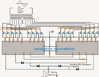
Referring to the image above, we can see how simply the 5 level cascaded inverter concept can be practically implemented using just a muti-tap transformer, a couple of 4017 ICs and 18 power BJTs, which could be easily replaced with mosfets if required.
Here a couple of 4017 ICs which are Johnsons 10 stage counter divider chips, are cascaded to produce a sequentially running or chasing logic highs across the shown pinouts of the ICs.
These sequentially running logic are used for triggering the connected power BJTs in the same sequence which in turn switch the transformer winding in an order which causes the transformer to produce a cascaded kind of sine equivalent waveform.
The transformer forms the heart of the circuit and employs a specially wounded primary with 11 taps. These taps are simply extracted uniformly from a single long calculated winding.
The BJTs associated with one of the ICs switch one of the halves of the transformer through 5 taps enabling the generation of 5 level steps, constituting one half cycle of the AC waveform, while the BJTs associated with the other ICs does the identical function to shape up the lower half AC cycle in the form of 5 level cascaded waveform.
The ICs are run by clock signals applied to the indicated position in the circuit, which could be acquired from any standard 555 IC astable circuit.
The first 5 sets of the BJTs build up the 5 levels of the waveform, the remaining 4 BJTs switch the same in reverse order to complete the cascaded waveform having a total of 9 skyscrapers.
These skyscrapers are formed by producing an ascending and descending voltage levels by the switching of the corresponding winding of the transformer which are rated at the relevant voltage levels
For example, winding #1 could be rated at 150V with respect to the center tap, the winding #2 at 200V, winding #3 at 230V, winding #4 at 270V and winding #5 at 330V, so when these are switched sequentially by the set of the shown 5 BJTs, we get the first 5 levels of the waveform, next when these winding are switched in reverse by the following 4 BJTs it creates the descending 4 level waveforms, thus completing the upper half cycle of the 220V AC.
The same is repeated by the other 9 BJTs associated with the other 4017 IC giving rise to the lower half of the 5 level cascaded AC, which completes one complete AC waveform of the required 220V AC output.
Transformer Details:

As may be witnessed in the above diagram, the transformer is an ordinary iron core type, made by winding the primary and the secondary with turns corresponding to the indicated voltage taps.
When connected with the corresponding BJTs these winding can be expected to induce a 5 level or a total of 9 level of cascaded waveform wherein the first 36V winding would correspond and induce a 150V, the 27V would induce an equivalent of 200V, while the 20V, 27V, 36V would be responsible of producing 230V, 270V and 330V across the secondary winding in the proposed cascaded format.
The set of taps on the lower side of the primary would carry out the switching to complete 4 ascending levels of the waveform.
An identical procedure would be repeated by the 9 BJTs associated with the complementary 4017 IC for building the negative half cycle of the AC...the negative is rendered due to the opposite orientation of the transformer winding with respect to the center tap.
Update:
Complete circuit diagram of the discussed multi-level cascaded sinewave inverter circuit
 The 1M pot associated with the 555 circuit will need to be adjusted for setting up a 50Hz or a 60Hz frequency for the inverter as per the country specs of the user.
Parts List
All unspecified resistors are 10k, 1/4 watt
All diodes are 1N4148
All BJTs are TIP142
ICs are 4017
In this website so far I have developed, designed and introduced many sine wave inverter circuits using straightforward concepts and ordinary components such as IC 555, which happen to be more result oriented instead of being complex and full of theoretical jumbles.
I have explained how simply a high power audio amplifier can be converted into a pure sine wave inverter, and I have also covered comprehensively regarding sine wave inveters using SPWM concept as given below:
Pure Sine Wave Inverter Circuit Using IC 4047
300 Watts PWM Controlled, Pure Sine Wave Inverter Circuit ...
Simple Pure Sine Wave Inverter Circuit - 500 Watt Pure Sine
Make this IC 556 Pure Sine Wave Inverter circuit
Sine Wave Inverter Circuit using Bubba Oscillator
We have also learned through this website regarding how to convert any square inverter into a pure sine wave inverter design.
Assessing the above sine wave inverter circuits using sine equivalent PWMs, we understand that the waveform of SPWMs do not directly match or coincide with an actual sinusoidal waveform, rather these execute the sine wave effect or results by interpreting the RMS value of the actual sine wave AC.
Although SPWM can be considered an effective way of replicating and implementing a reasonably pure sine wave, the fact that it does not simulate or coincide with a real sine wave makes the concept a little unsophisticated, especially if compared to a 5 Level cascaded sine wave inverter concept.
We can compare and analyze the two types of sine wave simulation concepts by referring to the following images:
We can clearly see that the 5 level cascaded concept produces a more obvious and effective simulation of a real sine wave than the SPWM concept which relies solely on matching the RMS value with the original sine wave magnitude.
Designing a conventional 5 Level Cascaded sine wave Inverter can be quite complex, but the concept which is explained here makes the implementation easier and employs ordinary components.
Referring to the image above, we can see how simply the 5 level cascaded inverter concept can be practically implemented using just a muti-tap transformer, a couple of 4017 ICs and 18 power BJTs, which could be easily replaced with mosfets if required.
Here a couple of 4017 ICs which are Johnsons 10 stage counter divider chips, are cascaded to produce a sequentially running or chasing logic highs across the shown pinouts of the ICs.
These sequentially running logic are used for triggering the connected power BJTs in the same sequence which in turn switch the transformer winding in an order which causes the transformer to produce a cascaded kind of sine equivalent waveform.
The transformer forms the heart of the circuit and employs a specially wounded primary with 11 taps. These taps are simply extracted uniformly from a single long calculated winding.
The BJTs associated with one of the ICs switch one of the halves of the transformer through 5 taps enabling the generation of 5 level steps, constituting one half cycle of the AC waveform, while the BJTs associated with the other ICs does the identical function to shape up the lower half AC cycle in the form of 5 level cascaded waveform.
The ICs are run by clock signals applied to the indicated position in the circuit, which could be acquired from any standard 555 IC astable circuit.
The first 5 sets of the BJTs build up the 5 levels of the waveform, the remaining 4 BJTs switch the same in reverse order to complete the cascaded waveform having a total of 9 skyscrapers.
These skyscrapers are formed by producing an ascending and descending voltage levels by the switching of the corresponding winding of the transformer which are rated at the relevant voltage levels
For example, winding #1 could be rated at 150V with respect to the center tap, the winding #2 at 200V, winding #3 at 230V, winding #4 at 270V and winding #5 at 330V, so when these are switched sequentially by the set of the shown 5 BJTs, we get the first 5 levels of the waveform, next when these winding are switched in reverse by the following 4 BJTs it creates the descending 4 level waveforms, thus completing the upper half cycle of the 220V AC.
The same is repeated by the other 9 BJTs associated with the other 4017 IC giving rise to the lower half of the 5 level cascaded AC, which completes one complete AC waveform of the required 220V AC output.
Transformer Details:
As may be witnessed in the above diagram, the transformer is an ordinary iron core type, made by winding the primary and the secondary with turns corresponding to the indicated voltage taps.
When connected with the corresponding BJTs these winding can be expected to induce a 5 level or a total of 9 level of cascaded waveform wherein the first 36V winding would correspond and induce a 150V, the 27V would induce an equivalent of 200V, while the 20V, 27V, 36V would be responsible of producing 230V, 270V and 330V across the secondary winding in the proposed cascaded format.
The set of taps on the lower side of the primary would carry out the switching to complete 4 ascending levels of the waveform.
An identical procedure would be repeated by the 9 BJTs associated with the complementary 4017 IC for building the negative half cycle of the AC...the negative is rendered due to the opposite orientation of the transformer winding with respect to the center tap.
Update:
Complete circuit diagram of the discussed multi-level cascaded sinewave inverter circuit
Parts List
All unspecified resistors are 10k, 1/4 watt
All diodes are 1N4148
All BJTs are TIP142
ICs are 4017
Available link for download
Subscribe to:
Posts (Atom)