Showing posts with label simple. Show all posts
Showing posts with label simple. Show all posts
Thursday, November 10, 2016
Simple Peak Detector Circuit
Simple Peak Detector Circuit
In this article we are going to learn about a peak detector circuit, its working principle and how to implement it in clap operated circuits for illuminating an LED in response to clap sounds.
By: Girish Radhakrishnan
A peak detector is a circuit which holds maximum amplitude value of a signal. If a signal varies rapidly and we are unable to measure it, then we go for peak detector. This circuit holds the maximum amplitude value for short period of time so that we can measure it.
There are many ways to do this and often used in many fields in electronics where rapid measurement is not viable.
For instance, taking heat gun thermometer as example, where the temperature of an object may vary rapidly at some situations, the peak value of temperature and current value of temperature is displayed simultaneously so that user can get an idea about the object.
Similarly, there are many situations in electronics, where we may need to measure peak signals.
Here, we are going to see simple peak detector circuit that consists of one diode, one capacitor and one resistor.
The diode permits the current in one direction, which is to charge the capacitor.
When the input drops the capacitor holds the value for a short period which gives some time to measure the peak. Here the short period could be ranging from a few milliseconds to a few seconds.
The values need to be refreshed time to time so that new values can be stored. To do this we need to discharge the capacitor. A bleed resistor is connected parallel to capacitor which discharges.

The capacitor discharge time can be calculated by the following formula:
T = 5 x C x R
Where, T is time in seconds
C is capacitance in Farad
R is resistance in Ohm
Clap Sensor circuit:
Here, we will implement the peak detector in a clap sensor circuit. This circuit responds to loud busts of sound such as clap.
There are three stages in this circuit, the microphone amplifier, peak detector and op-amp circuit that detects peak.
The sound gets converted to electrical signal by the microphone, gets amplified by op-amp. The amplified signal enters the peak detector circuit and charges the capacitor. The peak value stored in the capacitor becomes the peak input minus 0.7V for silicon diodes, since there will be always voltage drop across diode.

The value stored in the capacitor gets recognized by op-amp comparator circuit.
As soon as the peak value goes above reference voltage the LED turns ON.
As soon as the capacitor is discharged below reference voltage the LED turns OFF.
So, what was the role of peak detector in this circuit? Well, it holds the clap signal for few 100 milliseconds which helped the LED to stay illuminated for a few 100 milliseconds. If you wish LED to light longer, it can be done by incrementing capacitance and resistor values.
By: Girish Radhakrishnan
What is peak detector?
A peak detector is a circuit which holds maximum amplitude value of a signal. If a signal varies rapidly and we are unable to measure it, then we go for peak detector. This circuit holds the maximum amplitude value for short period of time so that we can measure it.
There are many ways to do this and often used in many fields in electronics where rapid measurement is not viable.
For instance, taking heat gun thermometer as example, where the temperature of an object may vary rapidly at some situations, the peak value of temperature and current value of temperature is displayed simultaneously so that user can get an idea about the object.
Similarly, there are many situations in electronics, where we may need to measure peak signals.
How it works?
Here, we are going to see simple peak detector circuit that consists of one diode, one capacitor and one resistor.
The diode permits the current in one direction, which is to charge the capacitor.
When the input drops the capacitor holds the value for a short period which gives some time to measure the peak. Here the short period could be ranging from a few milliseconds to a few seconds.
The values need to be refreshed time to time so that new values can be stored. To do this we need to discharge the capacitor. A bleed resistor is connected parallel to capacitor which discharges.
The capacitor discharge time can be calculated by the following formula:
T = 5 x C x R
Where, T is time in seconds
C is capacitance in Farad
R is resistance in Ohm
Clap Sensor circuit:
Here, we will implement the peak detector in a clap sensor circuit. This circuit responds to loud busts of sound such as clap.
There are three stages in this circuit, the microphone amplifier, peak detector and op-amp circuit that detects peak.
The sound gets converted to electrical signal by the microphone, gets amplified by op-amp. The amplified signal enters the peak detector circuit and charges the capacitor. The peak value stored in the capacitor becomes the peak input minus 0.7V for silicon diodes, since there will be always voltage drop across diode.
The value stored in the capacitor gets recognized by op-amp comparator circuit.
As soon as the peak value goes above reference voltage the LED turns ON.
As soon as the capacitor is discharged below reference voltage the LED turns OFF.
So, what was the role of peak detector in this circuit? Well, it holds the clap signal for few 100 milliseconds which helped the LED to stay illuminated for a few 100 milliseconds. If you wish LED to light longer, it can be done by incrementing capacitance and resistor values.
Available link for download

Thursday, November 3, 2016
Simple Vertical Axis Wind Turbine Generator Circuit
Simple Vertical Axis Wind Turbine Generator Circuit
The post explains a simple vertical axis wind turbine generator circuit using ready made high power generator dynamo and a vertical axis wind turbine mechanism. The idea was requested by Mr. Taibani.
The Request
Hello Swagatam,
Bro hope youre doing well.
Firstly thanks for all the great knowledge & information you have given here its really appreciated.
I am trying to do a project of home made low RPM VAWT generator which can generate enough power to run one small scale factory I need your help on winding section.
1) Correct copper winding design for low rpm.
2) Correct copper wire gauge.
3) Number of turns of winding.
4) What core material should be used for low drag ( Lenz effect ).
Please help me out & your readers with your great knowledge.
Thanks & Regards,
Taibani Imran.
The Design
Designing a VAWT motor is not easy and might require good expertise in the field and at the moment for me this looks much complex and I have little idea regarding the same.
However for any layman the idea could be easily implemented through a ready made generator as described below:
Below is an example of a 10,000 watt dynamo which could be used for the proposed vertical axis wind turbine generator application

Instead of winding a vertical axis wind generator yourself, a simpler idea would be to configure the VAWT mechanism with a high watt generator or a dynamo through a correctly calculated gear or pulley/belt ratio.
For example, the above shown 10 kv dynamo has a specifications of generating 10000 watt at around 3600 RPM, which implies that if the a pulley ratio of 1:100 is configured, the dynamo would be able to produce the rated amount of power with the VAWT rotating at just around 36 RPM, which could be achieved perhaps even at wind speeds as low as 5km per hour.
The following diagram shows a rough set up design for the above explained implementation:

The figure above shows a simple vertical axis wind turbine model, the vertical helical turbine is designed to capture wind flow on one half of its span while allow free flow on the other half, causing the propeller to initiate a rotational movement with high torque.
Being vertical in its positioning the VAWT does not rely on wind directions unlike the traditional horizontal axis wind turbines. This advantage makes the VAWT sustain its operations under all wind conditions regardless of its direction of flow.
The central vertical axis of the turbine can be seen attached with a gigantic flywheel, which is supposed to be a lot bigger than the wheel attached with the generator shaft.
The bigger the ratio, the bigger would be the conversion even at minimal wind speeds.
With a ratio of 1:100, the generator could be expected to be generating at its full capacity and specification, with the VAWT moving at a meager 50 RPM or even less. This speed could be in turn achieved at wind speeds not exceeding 5 to 10 miles per hour.
The above explained set up is for facilitating efficient conversions at low wind speeds, but what happens when the wind is rapid or during stormy conditions.
If this situation is not taken care of can easy rip-of the generator winding and burn it within no time.
In order to control the VAWT speed at dangerous wind speeds, the following shunt regulator circuit could be used with the output of the generator for achieving a constant speed on the generator and the VAWT.

In the above figure the generator output is applied to a high current triac shunt regulator network through a 50 amp bridge rectifier module.
The value of the zener diode determines the control threshold, which is shown as 220V in the diagram. It means under no circumstances the voltage from the generator can exceed the 220V mark, and if it does the excess power is simply shunted or shorted to ground via the triac.
This ensures a controlled rotation of the generator even at formidable wind speeds keeping the entire system stabilized and safe.
If the generator used is a 3 phase type of generator, the shunt regulator shown above could be replaced with a 3 phase shunt regulator using SCRs.
If you have any doubts regarding the discussed vertical axis wind turbine generator circuit, do feel free to express them through comments
The Request
Hello Swagatam,
Bro hope youre doing well.
Firstly thanks for all the great knowledge & information you have given here its really appreciated.
I am trying to do a project of home made low RPM VAWT generator which can generate enough power to run one small scale factory I need your help on winding section.
1) Correct copper winding design for low rpm.
2) Correct copper wire gauge.
3) Number of turns of winding.
4) What core material should be used for low drag ( Lenz effect ).
Please help me out & your readers with your great knowledge.
Thanks & Regards,
Taibani Imran.
The Design
Designing a VAWT motor is not easy and might require good expertise in the field and at the moment for me this looks much complex and I have little idea regarding the same.
However for any layman the idea could be easily implemented through a ready made generator as described below:
Below is an example of a 10,000 watt dynamo which could be used for the proposed vertical axis wind turbine generator application
Instead of winding a vertical axis wind generator yourself, a simpler idea would be to configure the VAWT mechanism with a high watt generator or a dynamo through a correctly calculated gear or pulley/belt ratio.
For example, the above shown 10 kv dynamo has a specifications of generating 10000 watt at around 3600 RPM, which implies that if the a pulley ratio of 1:100 is configured, the dynamo would be able to produce the rated amount of power with the VAWT rotating at just around 36 RPM, which could be achieved perhaps even at wind speeds as low as 5km per hour.
The following diagram shows a rough set up design for the above explained implementation:
The figure above shows a simple vertical axis wind turbine model, the vertical helical turbine is designed to capture wind flow on one half of its span while allow free flow on the other half, causing the propeller to initiate a rotational movement with high torque.
Being vertical in its positioning the VAWT does not rely on wind directions unlike the traditional horizontal axis wind turbines. This advantage makes the VAWT sustain its operations under all wind conditions regardless of its direction of flow.
The central vertical axis of the turbine can be seen attached with a gigantic flywheel, which is supposed to be a lot bigger than the wheel attached with the generator shaft.
The bigger the ratio, the bigger would be the conversion even at minimal wind speeds.
With a ratio of 1:100, the generator could be expected to be generating at its full capacity and specification, with the VAWT moving at a meager 50 RPM or even less. This speed could be in turn achieved at wind speeds not exceeding 5 to 10 miles per hour.
Controlling VAWT speed using Shunt Regulator Circuit
The above explained set up is for facilitating efficient conversions at low wind speeds, but what happens when the wind is rapid or during stormy conditions.
If this situation is not taken care of can easy rip-of the generator winding and burn it within no time.
In order to control the VAWT speed at dangerous wind speeds, the following shunt regulator circuit could be used with the output of the generator for achieving a constant speed on the generator and the VAWT.
In the above figure the generator output is applied to a high current triac shunt regulator network through a 50 amp bridge rectifier module.
The value of the zener diode determines the control threshold, which is shown as 220V in the diagram. It means under no circumstances the voltage from the generator can exceed the 220V mark, and if it does the excess power is simply shunted or shorted to ground via the triac.
This ensures a controlled rotation of the generator even at formidable wind speeds keeping the entire system stabilized and safe.
If the generator used is a 3 phase type of generator, the shunt regulator shown above could be replaced with a 3 phase shunt regulator using SCRs.
If you have any doubts regarding the discussed vertical axis wind turbine generator circuit, do feel free to express them through comments
Available link for download
Wednesday, November 2, 2016
Simple Refrigerator Protector Circuit
Simple Refrigerator Protector Circuit
This simple refrigerator protector circuit is actually a delay ON timer circuit which makes sure that whenever a power failure occurs or in case abrupt power fluctuations take place, the refrigerator is never allowed to switch ON instantly, rather after a delay of a few moments.
Today most modern refrigerators are equipped with a protection feature which prevents the fridge from suddenly switching ON or OFF due to sudden power fluctuations or a sudden power restoration.
However, for those fridges which are not equipped with this feature, the following simple delay ON timer circuit can be applied to enable the refrigerator to switch ON after a certain delay, and only when the mains power has become stable. Until this happens the circuit keeps the fridge switched OFF and monitors until the power has returned to a perfectly normal status.
Referring to the above shown refrigerator protection circuit, we are able to witness a two transistor circuit which forms a very basic yet effective delay ON timer circuit, meaning this circuit switches ON its output after some delay, after power is applied to it.
The power supply to the circuit is derived from the mains via a transformerless power supply circuit
which is appropriately stabilized at 12V and fed to the delay circuit.
Whenever power is switched ON, may it be during the first initialization, or during a power failure situation, the associated 1000uF capacitor prevents the BC547 from switching ON at the onset, which in turn keeps the BC557 and the triac switched OFF. The load is therefore unable to receive power and stays switched OFF too.
However, the 1000uF now gradually begins charging via the 330K resistor and when the potential difference across it reaches the approximate total of transistors biasing limit plus the emitter zener value (0.6 + 3 = 3.6V), the transistor begins switching ON which prompts the BC557 also to switch ON.
The triac now begins acquiring the required gate voltage and within moments switches ON the fridge.
The 1000uF capacitor stays charged as long as power is available to the circuit, and during power failures the capacitor discharges through the parallel 100k resistor so that it can get into the standby mode for the next delay ON cycle operation.
The time delay period can be accomplished by appropriately selecting the values of the 330K resistor, the 1000uF capacitor and the 3V zener diode, as per the users preference.
This concludes the explanation for the proposed simple refrigerator protection circuit, for any related query please feel free to use the comment box.
Today most modern refrigerators are equipped with a protection feature which prevents the fridge from suddenly switching ON or OFF due to sudden power fluctuations or a sudden power restoration.
However, for those fridges which are not equipped with this feature, the following simple delay ON timer circuit can be applied to enable the refrigerator to switch ON after a certain delay, and only when the mains power has become stable. Until this happens the circuit keeps the fridge switched OFF and monitors until the power has returned to a perfectly normal status.
 |
| WARNING: CIRCUIT IS NOT ISOLATED FROM MAINS... STRICT PRECAUTIONS MUST BE OBSERVED WHILE HANDLING THE DEVICE, WHILE ITS IN AN UNENCLOSED CONDITION. |
Referring to the above shown refrigerator protection circuit, we are able to witness a two transistor circuit which forms a very basic yet effective delay ON timer circuit, meaning this circuit switches ON its output after some delay, after power is applied to it.
The power supply to the circuit is derived from the mains via a transformerless power supply circuit
which is appropriately stabilized at 12V and fed to the delay circuit.
Whenever power is switched ON, may it be during the first initialization, or during a power failure situation, the associated 1000uF capacitor prevents the BC547 from switching ON at the onset, which in turn keeps the BC557 and the triac switched OFF. The load is therefore unable to receive power and stays switched OFF too.
However, the 1000uF now gradually begins charging via the 330K resistor and when the potential difference across it reaches the approximate total of transistors biasing limit plus the emitter zener value (0.6 + 3 = 3.6V), the transistor begins switching ON which prompts the BC557 also to switch ON.
The triac now begins acquiring the required gate voltage and within moments switches ON the fridge.
The 1000uF capacitor stays charged as long as power is available to the circuit, and during power failures the capacitor discharges through the parallel 100k resistor so that it can get into the standby mode for the next delay ON cycle operation.
The time delay period can be accomplished by appropriately selecting the values of the 330K resistor, the 1000uF capacitor and the 3V zener diode, as per the users preference.
This concludes the explanation for the proposed simple refrigerator protection circuit, for any related query please feel free to use the comment box.
Available link for download
Thursday, October 20, 2016
Simple LED Relay Changeover Emergency Lamp Circuit
Simple LED Relay Changeover Emergency Lamp Circuit
The post shows how to configure a simple LED relay changeover emergency light circuit using a battery back up which gets charged during mains presence and changes over to LED/battery mode as soon as mains fails. The idea was requested by one of the members of this blog.
The following discussion explains the application details for the proposed LED relay changeover emergency lamp circuit
Hi,
I am trying to make very simple changeover circuit.. where I am using a 12-0-12 Transformer to charge a 12v Motorcycle battery via mains.. when the mains go off the battery will power a 10w LED. But, the problem is the relay is not switching off, when the mains goes down.. Any ideas. Want to keep it really simple..
12VDC Relay / 2200uf-50v cap on Transformer.
Hi, make sure that the relay coil is connected with the rectified DC from the 12-0-12 transformer. The relay contacts should be only wired with the battery and the LED
Hi Swagatam,
Firstly Thanks for the Reply.
1. Yes the Relay Coil is connected with the Rectified DC.
2. If I connect the relay contacts to Battery / LED only, then how will the Battery get charged when Mains is ON? If i am not missing anything..
The Design

The above circuit is self explanatory and shows the configuration for implementing a simple LED relay changeover emergency lamp circuit.
The following discussion explains the application details for the proposed LED relay changeover emergency lamp circuit
Hi,
I am trying to make very simple changeover circuit.. where I am using a 12-0-12 Transformer to charge a 12v Motorcycle battery via mains.. when the mains go off the battery will power a 10w LED. But, the problem is the relay is not switching off, when the mains goes down.. Any ideas. Want to keep it really simple..
12VDC Relay / 2200uf-50v cap on Transformer.
Hi, make sure that the relay coil is connected with the rectified DC from the 12-0-12 transformer. The relay contacts should be only wired with the battery and the LED
Hi Swagatam,
Firstly Thanks for the Reply.
1. Yes the Relay Coil is connected with the Rectified DC.
2. If I connect the relay contacts to Battery / LED only, then how will the Battery get charged when Mains is ON? If i am not missing anything..
The Design
The above circuit is self explanatory and shows the configuration for implementing a simple LED relay changeover emergency lamp circuit.
Available link for download
Sunday, October 16, 2016
Simple Obstacle Avoiding Robot Circuit without Microcontroller
Simple Obstacle Avoiding Robot Circuit without Microcontroller
The post explains a simple obstacle avoiding robot circuit without microcontroller and without using special motor driver circuits or ICs. The idea was requested by Mr. Faiyyaz
The Request
Sir
Please send me circuit diagram for obstacles avoiding robot without microcontroller
Faiyyaz mulla
The Design
The operation is thus automatic without any manual or human intervention.
The presented idea of an obstacle avoiding robot without microcontroller as the name suggests does not employ a microcontroller and therefore is extremely simple to build and suitable to any new hobbyist.
While designing the circuit I realized that in order to implement the principle at least a couple of obstacles sensor modules would be required, because using a single module can cause erratic movement of the motor and may not help a smooth diversion or turning of the vehicle towards a free path.
The vehicle motor set up is quite similar to the remote control toy car which I had discussed in one of the earlier posts.
The following diagram represents one of the modules of the system, and therefore two or a pair of such modules would be required across the right and the left sides of the vehicle.
The idea is simple and works without microcontroller and without special motor driver ICs. That means you can make it without any kind of coding and without using any kind of complex motor driver IC.....and the circuit allows you to use any DC motor regardless of its power, so even high power obstacle avoiding vehicles could be made using this circuit which are normally used in malls and similar retail outlets.

Now lets try to understand the above circuit with the help of the following explanation:
The IC 555 is configured as an IR transmitter and is set to generate a constant 38kHz frequency, while the adjoining transistorized circuit is configured as the receiver stage or the IR sensor stage.
Lets assume its the right side module, and suppose this module happens to be the first to detect an obstacle in the path.
Therefore as soon as an obstacle is detected, the 38kHz frequency generated by the 555 IC is reflected towards the sensor of the adjoining receiver circuit.
The receiver instantly activates the associated transistors such that the final driver transistor is inhibited from conducting.
Now the motor which is controlled by this transistor is supposed to be located on the left side of the vehicle, that is on the opposite side of this module...similarly the motor located on the right side is actually controlled by the left side module.
Consequently, when the above assumed right hand side obstacle detector module activates, it stops the left hand side motor, while the right side motor is allowed to move normally.
This situation results in the vehicle being forced to take a left side diversion...which means now the assumed left module starts getting even more stronger obstacle signals and keeps forcing the vehicle to proceed harder on the ongoing diversion until it has completely avoided the obstacle. The module now stops receiving the obstacle signals and the vehicle begins moving ahead normally on its new path.
While the above diversion is carried out the left side module is forced to become more and more isolated and away from the obstacle so that it does not get an opportunity to interfere in the procedure, and allow a clean and smooth diversion of the vehicle.
Exactly the same procedures are implemented in case the left side module happens to sense the obstacle ahead of the right side module, wherein the vehicle is forced to move harder and harder toward the right side.
We can also see a "disabling" circuit stage in the module which are interconnected across the left and the right side modules. This stage is purposely introduced to ensure that both the modules are never activated together.
Therefore for example if the left side module becomes the first to detect an obstacle, it immediately disables the right side module and initiates the diversion of the vehicle on the right and vice versa.
The sensor IC could be an standard TSOP17XX series
For more info regarding the above sensor IC you can learn how to connect TSOP1738 IC
And the motor should be equipped with gear boxes so that the movement is originally maintained at a controlled level.
The complete set up of the left and right module and the associated electrical connections can be witnessed in the figure below:

Update
A little thinking tells us that the above simple obstacle avoiding robot circuit could also be implemented by using a single module, instead of the two.
However a single module would allow the vehicle to carry out a single sided diversion every time it detects an obstacle, therefore the system could be configured either to take a clockwise diversion or anticlockwise diversion depending on which motor is connected with the circuit for the actions.
The Request
Sir
Please send me circuit diagram for obstacles avoiding robot without microcontroller
Faiyyaz mulla
The Design
What is an Obstacle Avoiding Robot
Basically its in the form of a moving vehicle which is able to detect and avoid potential obstacles on its path and change its direction appropriately so that its motion stays uninterrupted, simple!
The operation is thus automatic without any manual or human intervention.
The presented idea of an obstacle avoiding robot without microcontroller as the name suggests does not employ a microcontroller and therefore is extremely simple to build and suitable to any new hobbyist.
While designing the circuit I realized that in order to implement the principle at least a couple of obstacles sensor modules would be required, because using a single module can cause erratic movement of the motor and may not help a smooth diversion or turning of the vehicle towards a free path.
The vehicle motor set up is quite similar to the remote control toy car which I had discussed in one of the earlier posts.
The following diagram represents one of the modules of the system, and therefore two or a pair of such modules would be required across the right and the left sides of the vehicle.
The idea is simple and works without microcontroller and without special motor driver ICs. That means you can make it without any kind of coding and without using any kind of complex motor driver IC.....and the circuit allows you to use any DC motor regardless of its power, so even high power obstacle avoiding vehicles could be made using this circuit which are normally used in malls and similar retail outlets.
Now lets try to understand the above circuit with the help of the following explanation:
The IC 555 is configured as an IR transmitter and is set to generate a constant 38kHz frequency, while the adjoining transistorized circuit is configured as the receiver stage or the IR sensor stage.
Lets assume its the right side module, and suppose this module happens to be the first to detect an obstacle in the path.
Therefore as soon as an obstacle is detected, the 38kHz frequency generated by the 555 IC is reflected towards the sensor of the adjoining receiver circuit.
The receiver instantly activates the associated transistors such that the final driver transistor is inhibited from conducting.
Now the motor which is controlled by this transistor is supposed to be located on the left side of the vehicle, that is on the opposite side of this module...similarly the motor located on the right side is actually controlled by the left side module.
Consequently, when the above assumed right hand side obstacle detector module activates, it stops the left hand side motor, while the right side motor is allowed to move normally.
This situation results in the vehicle being forced to take a left side diversion...which means now the assumed left module starts getting even more stronger obstacle signals and keeps forcing the vehicle to proceed harder on the ongoing diversion until it has completely avoided the obstacle. The module now stops receiving the obstacle signals and the vehicle begins moving ahead normally on its new path.
While the above diversion is carried out the left side module is forced to become more and more isolated and away from the obstacle so that it does not get an opportunity to interfere in the procedure, and allow a clean and smooth diversion of the vehicle.
Exactly the same procedures are implemented in case the left side module happens to sense the obstacle ahead of the right side module, wherein the vehicle is forced to move harder and harder toward the right side.
We can also see a "disabling" circuit stage in the module which are interconnected across the left and the right side modules. This stage is purposely introduced to ensure that both the modules are never activated together.
Therefore for example if the left side module becomes the first to detect an obstacle, it immediately disables the right side module and initiates the diversion of the vehicle on the right and vice versa.
The sensor IC could be an standard TSOP17XX series
For more info regarding the above sensor IC you can learn how to connect TSOP1738 IC
And the motor should be equipped with gear boxes so that the movement is originally maintained at a controlled level.
The complete set up of the left and right module and the associated electrical connections can be witnessed in the figure below:
Update
A little thinking tells us that the above simple obstacle avoiding robot circuit could also be implemented by using a single module, instead of the two.
However a single module would allow the vehicle to carry out a single sided diversion every time it detects an obstacle, therefore the system could be configured either to take a clockwise diversion or anticlockwise diversion depending on which motor is connected with the circuit for the actions.
Available link for download
Saturday, October 15, 2016
Simple 50 Watt Power Amplifier Circuit
Simple 50 Watt Power Amplifier Circuit
A simple 50 watt amplifier circuit is explained below, lets learn how to build it at home using this versatile single amplifier chip LM3876T
By: Dhrubajyoti Biswas
Analyzing the Circuit
A good power amplifier is a necessity, especially when it comes to listening music. An amplifier added to a sound system will definitely enrich the quality of music. This project therefore will attempt to give you a detailed insight of making a simple 50 watt power amplifier.
The system that we are going to deal with is primarily based upon the technical specification laid out by National Semiconductors, and following this the result came out well. Easy to build and good output in terms of distortion and noise, the following section will detail the way it is built.
Before we kick-start this development, we have tested the PCB and result came out positive. We have received very good sound quality provided the protection circuitry is not in operational mode.
The last stable version of the board ESP P19 (Rev-B) has few alterations, such as, the connection to the sound impairment monitor [SIM] has been taken out.
The following Figure is a layout of the original board:

As per the diagram, there is an addition of polyester bypass capacitors and the mute circuit is left disabled, since it is mainly useful when developing a preamp. However, we made some adjustment into the board to provide space for power and input connectors.
As per the above figure, the voltage gain is set to 27dB, and it can be changed by adding resistors of different value for the path of the feedback.
The inductor has 10 turns of enameled copper wire of 0.4mm and is wounded around the body of the 10ohm resistor. The soldered wire lies at the end of the resistor and the insulation should be brushed off on each end.
Our recommendation would be to use 1watt type 10ohm and 2.7ohm resistors. The rest should metal film of 1%. It is also ideal to keep the electrolytic capacitors @ 50V.
For supply, 100nF (0.1uF) should be placed near to the IC in order to avoid oscillation. The voltage supplies to maintain at full load should be around +/- 35 volts, which would produce 56 watts (Max.).
Also to achieve lowest case to the heatsink thermal resistance it is vital to engage max power. This can be done by mounting mica washer with no insulation. However, do keep in mind the heatsink need insulation from the chassis since the heatsink maintain supply voltage of –ve.
The following schematic in Figure shows the changes we made on the original board:

Referring to Figure above, the revised board is very much similar to that of the original one, except some changes by removing some components along with the SIM.
The present on-board decoupling gives great performance. It uses electrolytic of 100nF Polyester and 220uF electrolytic.
Alternatively, you can also use monolithic ceramic capacitor on every rail. While C1 and C2 is referred as polarized electrolytic types, you may use non-polarized electros.
Another option would be to apply on C1 a 1uF polyester cap. If C1 is intended to be used as tweeters you can use small values of 100nF which is good to go ahead.
If you are building the proposed simple 50 watt power amplifier circuit to use it for biamped/triamped system tweeter or midrange, the C1 valued need to be reduced to 100nF (3dB @ 72Hz).
Also you can use 1uF polyester at the rate of -3dB @ 7.2Hz in case of any general use. However, this adjustment would increase the performance of the bass and you can also apply any value till 10uF (approx.) on C1 if needed to do so.
The new design of the PCB facilitates using the amp as dual-mono. You can split the PCB track while each individual has its own power supply.
While the IMO carries less point, this enables cutting the PCB in half with each halves has its own supply. The board gives the facility to make output connection to the PCB pins, or by using PCB mount spade lug.
As per the board’s design shown in the figure, you can use LM3886. It is very much identical and moreover the specification is higher.
The PCB also have the provision to connect pin number 1 and 5. Furthermore, you can also use the board as a bridge in case of LM3886 to achieve 120W into 8ohms. Our suggestion would be to use P87B to enable out-oh-phase signal that is needed to operate BTL.
To run an amp as inverting is a common occurrence, but doing that ends up with low impedance to the preamp, which may give trouble as you may find distortion or problem in loading. Therefore, it is always safe to drive the amplifiers, since the P87B can drive each amp individually.
Whereas parallel operation is often a common suggestion when building this system, our experience in this domain does not recommend the same.
The requirements for gain tolerance during parallel operation is very strict as you need to ensure the amplifier matches 0.1% or keep it over the entire bandwidth.
Now since the impedance of the IC has low output, therefore even 100mV may end up generating high circulating currents via the IC’s. As 0.1? comes as usual suggestion, a mismatch of 100mV may end up 0.5A of circulating current, which ends up in overheating.

Figure above shows the IC pinouts for LM3876 where the pins are staggered to enable the PCB tracks run into the pin of the IC. The LM3886 on the other hand is very much identical to the former, and it can be used by adding little more power, if needed.
However, the only difference that lies between the two is in LM3886 it is mandatory for Pin 5 to connect to +ve supply.
The PCB used for this amp is mainly meant for stereo amplifier. It is single-sided with the location of supply fuse in the PCB. The stereo board contain small four fuses (115mm x 40 mm).
Overall the revised board as in Figure 1.1 is of the same size to that of the original (as shown in Figure 1.0) and we have applied similar spacing in between the IC’s to facilitate retro-fitting, if needed.
However, as a caution do keep in mind to use heat-sink for this project as the system gets really hot within a short time, which may end up destroying the things from overheating.
By: Dhrubajyoti Biswas
Analyzing the Circuit
A good power amplifier is a necessity, especially when it comes to listening music. An amplifier added to a sound system will definitely enrich the quality of music. This project therefore will attempt to give you a detailed insight of making a simple 50 watt power amplifier.
The system that we are going to deal with is primarily based upon the technical specification laid out by National Semiconductors, and following this the result came out well. Easy to build and good output in terms of distortion and noise, the following section will detail the way it is built.
Before we kick-start this development, we have tested the PCB and result came out positive. We have received very good sound quality provided the protection circuitry is not in operational mode.
The last stable version of the board ESP P19 (Rev-B) has few alterations, such as, the connection to the sound impairment monitor [SIM] has been taken out.
The following Figure is a layout of the original board:
As per the diagram, there is an addition of polyester bypass capacitors and the mute circuit is left disabled, since it is mainly useful when developing a preamp. However, we made some adjustment into the board to provide space for power and input connectors.
As per the above figure, the voltage gain is set to 27dB, and it can be changed by adding resistors of different value for the path of the feedback.
The inductor has 10 turns of enameled copper wire of 0.4mm and is wounded around the body of the 10ohm resistor. The soldered wire lies at the end of the resistor and the insulation should be brushed off on each end.
Our recommendation would be to use 1watt type 10ohm and 2.7ohm resistors. The rest should metal film of 1%. It is also ideal to keep the electrolytic capacitors @ 50V.
For supply, 100nF (0.1uF) should be placed near to the IC in order to avoid oscillation. The voltage supplies to maintain at full load should be around +/- 35 volts, which would produce 56 watts (Max.).
Also to achieve lowest case to the heatsink thermal resistance it is vital to engage max power. This can be done by mounting mica washer with no insulation. However, do keep in mind the heatsink need insulation from the chassis since the heatsink maintain supply voltage of –ve.
The following schematic in Figure shows the changes we made on the original board:
Referring to Figure above, the revised board is very much similar to that of the original one, except some changes by removing some components along with the SIM.
The present on-board decoupling gives great performance. It uses electrolytic of 100nF Polyester and 220uF electrolytic.
Alternatively, you can also use monolithic ceramic capacitor on every rail. While C1 and C2 is referred as polarized electrolytic types, you may use non-polarized electros.
Another option would be to apply on C1 a 1uF polyester cap. If C1 is intended to be used as tweeters you can use small values of 100nF which is good to go ahead.
If you are building the proposed simple 50 watt power amplifier circuit to use it for biamped/triamped system tweeter or midrange, the C1 valued need to be reduced to 100nF (3dB @ 72Hz).
Also you can use 1uF polyester at the rate of -3dB @ 7.2Hz in case of any general use. However, this adjustment would increase the performance of the bass and you can also apply any value till 10uF (approx.) on C1 if needed to do so.
The new design of the PCB facilitates using the amp as dual-mono. You can split the PCB track while each individual has its own power supply.
While the IMO carries less point, this enables cutting the PCB in half with each halves has its own supply. The board gives the facility to make output connection to the PCB pins, or by using PCB mount spade lug.
As per the board’s design shown in the figure, you can use LM3886. It is very much identical and moreover the specification is higher.
The PCB also have the provision to connect pin number 1 and 5. Furthermore, you can also use the board as a bridge in case of LM3886 to achieve 120W into 8ohms. Our suggestion would be to use P87B to enable out-oh-phase signal that is needed to operate BTL.
To run an amp as inverting is a common occurrence, but doing that ends up with low impedance to the preamp, which may give trouble as you may find distortion or problem in loading. Therefore, it is always safe to drive the amplifiers, since the P87B can drive each amp individually.
Whereas parallel operation is often a common suggestion when building this system, our experience in this domain does not recommend the same.
The requirements for gain tolerance during parallel operation is very strict as you need to ensure the amplifier matches 0.1% or keep it over the entire bandwidth.
Now since the impedance of the IC has low output, therefore even 100mV may end up generating high circulating currents via the IC’s. As 0.1? comes as usual suggestion, a mismatch of 100mV may end up 0.5A of circulating current, which ends up in overheating.
Figure above shows the IC pinouts for LM3876 where the pins are staggered to enable the PCB tracks run into the pin of the IC. The LM3886 on the other hand is very much identical to the former, and it can be used by adding little more power, if needed.
However, the only difference that lies between the two is in LM3886 it is mandatory for Pin 5 to connect to +ve supply.
The PCB used for this amp is mainly meant for stereo amplifier. It is single-sided with the location of supply fuse in the PCB. The stereo board contain small four fuses (115mm x 40 mm).
Overall the revised board as in Figure 1.1 is of the same size to that of the original (as shown in Figure 1.0) and we have applied similar spacing in between the IC’s to facilitate retro-fitting, if needed.
However, as a caution do keep in mind to use heat-sink for this project as the system gets really hot within a short time, which may end up destroying the things from overheating.
Available link for download
Saturday, October 1, 2016
Simple Surround Sound Decoder Circuit
Simple Surround Sound Decoder Circuit
This article is written with an intent to explain in detail behind the making of a simple surround-sound decoder circuit.
By: Dhrubajyoti Biswas
The concept of the decoder was first introduced by David Hafler in the 70s. His research illustrates the way to use two speakers as rear speakers on a surround system.
The figure below is a diagram based on Hafler’s research:
According to Figure 1, Hafler designed the circuit to enable the rear speakers generate the difference of signal between right and left output.
While every stereo encoded system maintains difference of signal between the right and left channel, it is that difference of signal when received by the rear speakers gets reproduced.
However, it is vital to keep in mind not to earth the negative terminals of the rear speakers, else the rear will behave parallel to the main front speakers.
Line Level Passive Version
Using individual amplifier for rear speakers is not actually possible. However, there is a way-out which we figured out after some research. Referring to Figure 2, it is totally passive, but it needs an ideal transformer – a transformer with impedance of 10K [1:1 ratio], which is quite rare to find, but available.
As an alternative we have tried using a 600ohm unit. But it is for the impedance the output we received was not good as it lacks bass.
However, upon loading the transformer, it increased the bass quality but the preamp doesn’t seem to work at its fullest because of the impedance. It is for this reason that we have used telephonic transformers with 600:600ohms, and it worked well.
The circuit in Figure 2 illustrates the way we followed. Following this design, it worked, but it has very low impedance on all cases barring solid-state preamp.
Using 600ohm unit, the loss generated is around 3dB. The low frequency is -3dB on 100Hz. However, it varies based upon the quality of the transformer.
600ohm telephony transformer is widely available in the market, but many of them are not up to the mark to use it in this experiment.
Most of the hi-powered transformers are sold in bulk and is therefore hard to procure a single copy. So, the alternative would be to use dual opamp to design the system, and its process is mentioned below in detail.
Explaining the New Circuit
The schematic diagram in Figure 3 gives a detailed view behind this development of the simple surround sound decoder circuit.
While the new design [Figure 3] will follow Hafler’s principle, this new circuit has simplified wiring, albeit we needed extra power amps. There is now a center channel signal and the sub-woofer to receive mono signal is also set.
You may have encountered similar type of circuit on other papers, but there are some twists into it. We avoided any active electronics on left/right channels and introduced opamps to zero down the factor that may cause degradation of sound.
The 50K impedance will not pose any barrier for a preamp, as the main signal is parallel to the additional circuit.
Extra volume control has been excluded from the system, because of the presence of volume control in the preamp. Moreover, the power amp of rear channel also has level control to balance the front and rear levels.
Please note, if you are following the circuit as in Figure 3 do ensure to make the rear speakers wired-out phase.
Let one speaker connect to the amp on a normal fashion and the second should be connected keeping the leads of speaker reversed.
Though the difference maybe negligible, but to derive the best quality effect it is always advisable to opt for out-of-phase connection. This helps in maintaining left-right and right-left signals.
The way surround sound decoder circuit works
A1 opamp should be connected in the form of subtracting amplifier, and if same signal is passed to both speakers, the result will be Zero.
This will result to removal of all information that are common from the stereo signal, and would produce the difference signal, similar to that of Hafler’s. A2 on the other hand is a summing amplifier. Its output has all necessary information from the left and right channels.
Center Channel Control
VR1 pot is set to level the center channel. It can either be a conventional pot or trimpot with the rear mounted.
Adding up the two channels [left / right channel] where signal is not mono, -3dB will be will be the level of center channel.
For instance, if the center channel speech is mono then the level becomes equal on both speakers. The possibility of amp overloading or the speaker is a rare case here, since the speakers and channel amplifier are not as much powerful compared to the left/right channels.
The sound of center channel does not need to be high. It has to be stable and the available level control is quite enough to generate required output.
The use of C1 Capacitor is not mandatory as it provides roll-off frequency of 8kHz. This actually helps to reduce any issues on the signal of the main stereo.
Output – Sub-Woofer
The output of the sub-woofer is taken from central channel mixer and added no-pass filter because it is hard to determine a sub where there is already a filter.
Other factors
100ohms resistors are used to block the oscillation of opamps by preventing the capacitance of the signal lead. Following this would not result to loss in frequency, but if you use 100m long signal leads, it may pose problem.
Referring to Figure 3, the rear speakers have two outputs in parallel.
The reason to do it is to enable easy wiring to facilitate connection of stereo amplifier with the rear speakers.
Normally, mono amplifier would do fine as long as it drives parallel to the two rear speakers. But this may not be feasible if you are using 4ohm speakers and if you do use it then ensure to connect them in the form of series. In order to enable out-of-phase connection, the red terminals need to get joined, and further connect the terminal of the speakers to the output of the amplifier.
Building the System
You can place the entire system on a metal case. Using metal case blocks the hum or other noise coming from mains etc.
While there is no factor of heat generation, you can use small case. However, ensure to maintain space to fit the RCA connectors and rest of the components.
Also, be sure to not to set the components loose as this may lead to short circuit.
You can wire the components and the dual opamp on a Veroboard. Also do ensure to apply 1% metal film all over it to lower the noise.
You may keep the RCA connectors hard-wired. Do ensure to check the earthing.
The power supply center lap and the RCA connectors should maintain secure connection to avoid noise pickup. You can also use 100uF polyester caps to connect with 100uF supply bypass capacitors in parallel, but this is not mandatory.
Delay Line
If you are planning to enrich the sound you can also apply delay line in order to delay the sound going into the rear speakers. But that is again not mandatory.
Overall, performance of your system is fully dependent on the way you have arranged the circuit. If the proposed simple surround sound decoder circuit is not well built you may face constant issues compared to a well-built one.
By: Dhrubajyoti Biswas
The concept of the decoder was first introduced by David Hafler in the 70s. His research illustrates the way to use two speakers as rear speakers on a surround system.
The figure below is a diagram based on Hafler’s research:
 |
| Figure 1 |
According to Figure 1, Hafler designed the circuit to enable the rear speakers generate the difference of signal between right and left output.
While every stereo encoded system maintains difference of signal between the right and left channel, it is that difference of signal when received by the rear speakers gets reproduced.
However, it is vital to keep in mind not to earth the negative terminals of the rear speakers, else the rear will behave parallel to the main front speakers.
Line Level Passive Version
Using individual amplifier for rear speakers is not actually possible. However, there is a way-out which we figured out after some research. Referring to Figure 2, it is totally passive, but it needs an ideal transformer – a transformer with impedance of 10K [1:1 ratio], which is quite rare to find, but available.
 |
| Figure 2 |
As an alternative we have tried using a 600ohm unit. But it is for the impedance the output we received was not good as it lacks bass.
However, upon loading the transformer, it increased the bass quality but the preamp doesn’t seem to work at its fullest because of the impedance. It is for this reason that we have used telephonic transformers with 600:600ohms, and it worked well.
The circuit in Figure 2 illustrates the way we followed. Following this design, it worked, but it has very low impedance on all cases barring solid-state preamp.
Using 600ohm unit, the loss generated is around 3dB. The low frequency is -3dB on 100Hz. However, it varies based upon the quality of the transformer.
600ohm telephony transformer is widely available in the market, but many of them are not up to the mark to use it in this experiment.
Most of the hi-powered transformers are sold in bulk and is therefore hard to procure a single copy. So, the alternative would be to use dual opamp to design the system, and its process is mentioned below in detail.
Explaining the New Circuit
The schematic diagram in Figure 3 gives a detailed view behind this development of the simple surround sound decoder circuit.
 |
| Figure 3 |
While the new design [Figure 3] will follow Hafler’s principle, this new circuit has simplified wiring, albeit we needed extra power amps. There is now a center channel signal and the sub-woofer to receive mono signal is also set.
You may have encountered similar type of circuit on other papers, but there are some twists into it. We avoided any active electronics on left/right channels and introduced opamps to zero down the factor that may cause degradation of sound.
The 50K impedance will not pose any barrier for a preamp, as the main signal is parallel to the additional circuit.
Extra volume control has been excluded from the system, because of the presence of volume control in the preamp. Moreover, the power amp of rear channel also has level control to balance the front and rear levels.
Please note, if you are following the circuit as in Figure 3 do ensure to make the rear speakers wired-out phase.
Let one speaker connect to the amp on a normal fashion and the second should be connected keeping the leads of speaker reversed.
Though the difference maybe negligible, but to derive the best quality effect it is always advisable to opt for out-of-phase connection. This helps in maintaining left-right and right-left signals.
The way surround sound decoder circuit works
A1 opamp should be connected in the form of subtracting amplifier, and if same signal is passed to both speakers, the result will be Zero.
This will result to removal of all information that are common from the stereo signal, and would produce the difference signal, similar to that of Hafler’s. A2 on the other hand is a summing amplifier. Its output has all necessary information from the left and right channels.
Center Channel Control
VR1 pot is set to level the center channel. It can either be a conventional pot or trimpot with the rear mounted.
Adding up the two channels [left / right channel] where signal is not mono, -3dB will be will be the level of center channel.
For instance, if the center channel speech is mono then the level becomes equal on both speakers. The possibility of amp overloading or the speaker is a rare case here, since the speakers and channel amplifier are not as much powerful compared to the left/right channels.
The sound of center channel does not need to be high. It has to be stable and the available level control is quite enough to generate required output.
The use of C1 Capacitor is not mandatory as it provides roll-off frequency of 8kHz. This actually helps to reduce any issues on the signal of the main stereo.
Output – Sub-Woofer
The output of the sub-woofer is taken from central channel mixer and added no-pass filter because it is hard to determine a sub where there is already a filter.
Other factors
100ohms resistors are used to block the oscillation of opamps by preventing the capacitance of the signal lead. Following this would not result to loss in frequency, but if you use 100m long signal leads, it may pose problem.
Referring to Figure 3, the rear speakers have two outputs in parallel.
The reason to do it is to enable easy wiring to facilitate connection of stereo amplifier with the rear speakers.
Normally, mono amplifier would do fine as long as it drives parallel to the two rear speakers. But this may not be feasible if you are using 4ohm speakers and if you do use it then ensure to connect them in the form of series. In order to enable out-of-phase connection, the red terminals need to get joined, and further connect the terminal of the speakers to the output of the amplifier.
Building the System
You can place the entire system on a metal case. Using metal case blocks the hum or other noise coming from mains etc.
While there is no factor of heat generation, you can use small case. However, ensure to maintain space to fit the RCA connectors and rest of the components.
Also, be sure to not to set the components loose as this may lead to short circuit.
You can wire the components and the dual opamp on a Veroboard. Also do ensure to apply 1% metal film all over it to lower the noise.
You may keep the RCA connectors hard-wired. Do ensure to check the earthing.
The power supply center lap and the RCA connectors should maintain secure connection to avoid noise pickup. You can also use 100uF polyester caps to connect with 100uF supply bypass capacitors in parallel, but this is not mandatory.
Delay Line
If you are planning to enrich the sound you can also apply delay line in order to delay the sound going into the rear speakers. But that is again not mandatory.
Overall, performance of your system is fully dependent on the way you have arranged the circuit. If the proposed simple surround sound decoder circuit is not well built you may face constant issues compared to a well-built one.
Available link for download
Thursday, September 29, 2016
Simple 5 Level Cascaded Sine Wave Inverter Circuit
Simple 5 Level Cascaded Sine Wave Inverter Circuit
In this article we learn how to make a multilevel (5 level) cascaded inverter circuit using a very simple concept developed by me. Lets learn more regarding the details.
In this website so far I have developed, designed and introduced many sine wave inverter circuits using straightforward concepts and ordinary components such as IC 555, which happen to be more result oriented instead of being complex and full of theoretical jumbles.
I have explained how simply a high power audio amplifier can be converted into a pure sine wave inverter, and I have also covered comprehensively regarding sine wave inveters using SPWM concept as given below:
Pure Sine Wave Inverter Circuit Using IC 4047
300 Watts PWM Controlled, Pure Sine Wave Inverter Circuit ...
Simple Pure Sine Wave Inverter Circuit - 500 Watt Pure Sine
Make this IC 556 Pure Sine Wave Inverter circuit
Sine Wave Inverter Circuit using Bubba Oscillator
We have also learned through this website regarding how to convert any square inverter into a pure sine wave inverter design.
Assessing the above sine wave inverter circuits using sine equivalent PWMs, we understand that the waveform of SPWMs do not directly match or coincide with an actual sinusoidal waveform, rather these execute the sine wave effect or results by interpreting the RMS value of the actual sine wave AC.
Although SPWM can be considered an effective way of replicating and implementing a reasonably pure sine wave, the fact that it does not simulate or coincide with a real sine wave makes the concept a little unsophisticated, especially if compared to a 5 Level cascaded sine wave inverter concept.
We can compare and analyze the two types of sine wave simulation concepts by referring to the following images:

We can clearly see that the 5 level cascaded concept produces a more obvious and effective simulation of a real sine wave than the SPWM concept which relies solely on matching the RMS value with the original sine wave magnitude.
Designing a conventional 5 Level Cascaded sine wave Inverter can be quite complex, but the concept which is explained here makes the implementation easier and employs ordinary components.
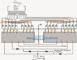
Referring to the image above, we can see how simply the 5 level cascaded inverter concept can be practically implemented using just a muti-tap transformer, a couple of 4017 ICs and 18 power BJTs, which could be easily replaced with mosfets if required.
Here a couple of 4017 ICs which are Johnsons 10 stage counter divider chips, are cascaded to produce a sequentially running or chasing logic highs across the shown pinouts of the ICs.
These sequentially running logic are used for triggering the connected power BJTs in the same sequence which in turn switch the transformer winding in an order which causes the transformer to produce a cascaded kind of sine equivalent waveform.
The transformer forms the heart of the circuit and employs a specially wounded primary with 11 taps. These taps are simply extracted uniformly from a single long calculated winding.
The BJTs associated with one of the ICs switch one of the halves of the transformer through 5 taps enabling the generation of 5 level steps, constituting one half cycle of the AC waveform, while the BJTs associated with the other ICs does the identical function to shape up the lower half AC cycle in the form of 5 level cascaded waveform.
The ICs are run by clock signals applied to the indicated position in the circuit, which could be acquired from any standard 555 IC astable circuit.
The first 5 sets of the BJTs build up the 5 levels of the waveform, the remaining 4 BJTs switch the same in reverse order to complete the cascaded waveform having a total of 9 skyscrapers.
These skyscrapers are formed by producing an ascending and descending voltage levels by the switching of the corresponding winding of the transformer which are rated at the relevant voltage levels
For example, winding #1 could be rated at 150V with respect to the center tap, the winding #2 at 200V, winding #3 at 230V, winding #4 at 270V and winding #5 at 330V, so when these are switched sequentially by the set of the shown 5 BJTs, we get the first 5 levels of the waveform, next when these winding are switched in reverse by the following 4 BJTs it creates the descending 4 level waveforms, thus completing the upper half cycle of the 220V AC.
The same is repeated by the other 9 BJTs associated with the other 4017 IC giving rise to the lower half of the 5 level cascaded AC, which completes one complete AC waveform of the required 220V AC output.
Transformer Details:

As may be witnessed in the above diagram, the transformer is an ordinary iron core type, made by winding the primary and the secondary with turns corresponding to the indicated voltage taps.
When connected with the corresponding BJTs these winding can be expected to induce a 5 level or a total of 9 level of cascaded waveform wherein the first 36V winding would correspond and induce a 150V, the 27V would induce an equivalent of 200V, while the 20V, 27V, 36V would be responsible of producing 230V, 270V and 330V across the secondary winding in the proposed cascaded format.
The set of taps on the lower side of the primary would carry out the switching to complete 4 ascending levels of the waveform.
An identical procedure would be repeated by the 9 BJTs associated with the complementary 4017 IC for building the negative half cycle of the AC...the negative is rendered due to the opposite orientation of the transformer winding with respect to the center tap.
Update:
Complete circuit diagram of the discussed multi-level cascaded sinewave inverter circuit
 The 1M pot associated with the 555 circuit will need to be adjusted for setting up a 50Hz or a 60Hz frequency for the inverter as per the country specs of the user.
Parts List
All unspecified resistors are 10k, 1/4 watt
All diodes are 1N4148
All BJTs are TIP142
ICs are 4017
In this website so far I have developed, designed and introduced many sine wave inverter circuits using straightforward concepts and ordinary components such as IC 555, which happen to be more result oriented instead of being complex and full of theoretical jumbles.
I have explained how simply a high power audio amplifier can be converted into a pure sine wave inverter, and I have also covered comprehensively regarding sine wave inveters using SPWM concept as given below:
Pure Sine Wave Inverter Circuit Using IC 4047
300 Watts PWM Controlled, Pure Sine Wave Inverter Circuit ...
Simple Pure Sine Wave Inverter Circuit - 500 Watt Pure Sine
Make this IC 556 Pure Sine Wave Inverter circuit
Sine Wave Inverter Circuit using Bubba Oscillator
We have also learned through this website regarding how to convert any square inverter into a pure sine wave inverter design.
Assessing the above sine wave inverter circuits using sine equivalent PWMs, we understand that the waveform of SPWMs do not directly match or coincide with an actual sinusoidal waveform, rather these execute the sine wave effect or results by interpreting the RMS value of the actual sine wave AC.
Although SPWM can be considered an effective way of replicating and implementing a reasonably pure sine wave, the fact that it does not simulate or coincide with a real sine wave makes the concept a little unsophisticated, especially if compared to a 5 Level cascaded sine wave inverter concept.
We can compare and analyze the two types of sine wave simulation concepts by referring to the following images:
We can clearly see that the 5 level cascaded concept produces a more obvious and effective simulation of a real sine wave than the SPWM concept which relies solely on matching the RMS value with the original sine wave magnitude.
Designing a conventional 5 Level Cascaded sine wave Inverter can be quite complex, but the concept which is explained here makes the implementation easier and employs ordinary components.
Referring to the image above, we can see how simply the 5 level cascaded inverter concept can be practically implemented using just a muti-tap transformer, a couple of 4017 ICs and 18 power BJTs, which could be easily replaced with mosfets if required.
Here a couple of 4017 ICs which are Johnsons 10 stage counter divider chips, are cascaded to produce a sequentially running or chasing logic highs across the shown pinouts of the ICs.
These sequentially running logic are used for triggering the connected power BJTs in the same sequence which in turn switch the transformer winding in an order which causes the transformer to produce a cascaded kind of sine equivalent waveform.
The transformer forms the heart of the circuit and employs a specially wounded primary with 11 taps. These taps are simply extracted uniformly from a single long calculated winding.
The BJTs associated with one of the ICs switch one of the halves of the transformer through 5 taps enabling the generation of 5 level steps, constituting one half cycle of the AC waveform, while the BJTs associated with the other ICs does the identical function to shape up the lower half AC cycle in the form of 5 level cascaded waveform.
The ICs are run by clock signals applied to the indicated position in the circuit, which could be acquired from any standard 555 IC astable circuit.
The first 5 sets of the BJTs build up the 5 levels of the waveform, the remaining 4 BJTs switch the same in reverse order to complete the cascaded waveform having a total of 9 skyscrapers.
These skyscrapers are formed by producing an ascending and descending voltage levels by the switching of the corresponding winding of the transformer which are rated at the relevant voltage levels
For example, winding #1 could be rated at 150V with respect to the center tap, the winding #2 at 200V, winding #3 at 230V, winding #4 at 270V and winding #5 at 330V, so when these are switched sequentially by the set of the shown 5 BJTs, we get the first 5 levels of the waveform, next when these winding are switched in reverse by the following 4 BJTs it creates the descending 4 level waveforms, thus completing the upper half cycle of the 220V AC.
The same is repeated by the other 9 BJTs associated with the other 4017 IC giving rise to the lower half of the 5 level cascaded AC, which completes one complete AC waveform of the required 220V AC output.
Transformer Details:
As may be witnessed in the above diagram, the transformer is an ordinary iron core type, made by winding the primary and the secondary with turns corresponding to the indicated voltage taps.
When connected with the corresponding BJTs these winding can be expected to induce a 5 level or a total of 9 level of cascaded waveform wherein the first 36V winding would correspond and induce a 150V, the 27V would induce an equivalent of 200V, while the 20V, 27V, 36V would be responsible of producing 230V, 270V and 330V across the secondary winding in the proposed cascaded format.
The set of taps on the lower side of the primary would carry out the switching to complete 4 ascending levels of the waveform.
An identical procedure would be repeated by the 9 BJTs associated with the complementary 4017 IC for building the negative half cycle of the AC...the negative is rendered due to the opposite orientation of the transformer winding with respect to the center tap.
Update:
Complete circuit diagram of the discussed multi-level cascaded sinewave inverter circuit
Parts List
All unspecified resistors are 10k, 1/4 watt
All diodes are 1N4148
All BJTs are TIP142
ICs are 4017
Available link for download
Tuesday, September 27, 2016
Simple 20 watt Amplifier Circuit
Simple 20 watt Amplifier Circuit
This article is written with an intent to build a simple 20 Watt Amplifier
By: Dhrubajyoti Biswas
A single-ended Class-A amplifier is probably one of the best example when it comes to solid-state single-ended output. On the other hand, the passive load can be a transformer, resistor or an amplifier as in this case, and a current sink. Here we have used a cheap current sink having high linearity, which is good to go with this project.
For many electrical engineers it is often seen that they recommend using 1:1 transformers or inductors. But we will avoid that process because both the component is quite expensive and need high precision, else it may have reverse effect on the loss of quality of the sound. The drop of sound quality is mainly because it is non-linear and frequency dependent.
In this experiment we have used a basic circuitry – a 60watt power amp, with the facility to modify it to operate well with Class-A. It is to my knowledge that many have tried this approach to build the amplifier and the results turned out positive. Further, we have used +/- 20volts electric supply. It can be either regulated, conventional or even applying a capacitance multiplier and moreover before clipping, it should have its capability of around 22 watts. So it is advisable to use a bigger heat-sink as there are high chance of the amplifier getting hot.
In our previous experiment constructing the amplifier we have applied quiescent current of 3A. Here we reduced it to 2.6A, with an intent to reduce dissipation of watt. But still it will release at least 110W from each amplifier.
Using either big plastic case device or TO-3 transistors is highly recommended, because the heat transfer is one the biggest challenge that you may have to face building this amp. Also we recommend using separate dissipation for individual transistor. This will enable generation of low thermal resistance.
You can also use a bigger transistor for this development, but that would be pricey. Therefore, considering the pocket it is always better to use two parallel transistors. They are cheaper compared to big transistors albeit maintaining the quality.
Following is the schematic diagram of the simple 20 watt amplifier circuit to help building the system.

20W Class-A Amplifier Circuit
The sink shown here in the diagram is built on the similar concept to that of the output stages. 4x1ohm 1W resistors [0.25ohm] are placed in parallel. However, it may need some experimentation as the current gets determined by the base-emitter voltage BC549. The way the circuit works, BC549 will fetch base current that are in excess from the resistors. As the voltage exceeds to 0.65V across the resistors, the transistor starts and further adjusts balance. Furthermore, you can also set the DC offset using 1K trimpot to manage the LTP.
Optimum Current
Ideally the Class-A amplifier should maintain operating current 110% more than the peak current of the speaker. So a loudspeaker with an impedance of 8ohm and +/-22V supply of current, the maximum current of the speaker will be:
I = V/R = 22/8 = 2.75A.
The above calculation does not indicate the loss of current during output. It is definite that there will be loss of 3 volts in the output of the circuit, which is based on the loss in the emitter or driver resistors and the loss in output device.
The maximum voltage therefore is 2.375A @ 8ohms = 19V peak. Now by adding fudge factor to 110% the operating current is 2.6125A (2.6A approx.), and following this, the output power would be 22.5W.
However, it is important to note that whereas –ve supply is constant, the +ve on the other hand varies from the available steady current. With high signals the current gets doubled as the upper transistor turns on or for negative peaks it will go down to zero. This situation is a common occurrence on Class-A amplifier [single-ended] and it makes the power-supply design complex.
Adjust Quiescent Current
If the current sense resistor is more than optimal then you can use trimpot and wiper to the base of BC549 for accurate current flow. However, do keep in mind to maintain distance between the sense resistor from those that generate high source, for example, power resistors. Maintaining no safe distance will lead the current to drop with the amp getting hotter.
Be cautious when using the trimpot, since the wiper is wounded to supply line of -35V. A wrong move here may damage the trimpot. Therefore, initiate with the wiper at the collector of the output devices. Slowly increase the current till it reaches the required setting. You can also use multi-turn pot as an alternative, which would be the best.
The following diagram shows making of a current sink variable for the proposed 20 watt amplifier circuit.

Variable Current Source
The use of 1K resistors as per figure is to ensure not to sink infinite current even when pot turns into an open circuit. Also it is necessary to give time [10 minutes or more at times] to stabilize the temperature across the heat-sink. However, the time to reach the operating temperature may vary based upon the size of the heat-sink, as bigger heat-sink comes with higher thermal mass and thus it takes time.
Heat-sink is one of the most vital components on a Class-A design. It is therefore mandatory to use a sink that would have thermal rating, which is less than 0.5°C/Watt. Consider a situation when the dissipation is about quiescent 110W, a heat-sink with the said specification will have 55°C rise in temperature, and the transistors on 80°C which eventually makes it hot. You can use thermal rating of 0.25°C, but there won’t be much effect on generated heat.
By: Dhrubajyoti Biswas
A single-ended Class-A amplifier is probably one of the best example when it comes to solid-state single-ended output. On the other hand, the passive load can be a transformer, resistor or an amplifier as in this case, and a current sink. Here we have used a cheap current sink having high linearity, which is good to go with this project.
For many electrical engineers it is often seen that they recommend using 1:1 transformers or inductors. But we will avoid that process because both the component is quite expensive and need high precision, else it may have reverse effect on the loss of quality of the sound. The drop of sound quality is mainly because it is non-linear and frequency dependent.
In this experiment we have used a basic circuitry – a 60watt power amp, with the facility to modify it to operate well with Class-A. It is to my knowledge that many have tried this approach to build the amplifier and the results turned out positive. Further, we have used +/- 20volts electric supply. It can be either regulated, conventional or even applying a capacitance multiplier and moreover before clipping, it should have its capability of around 22 watts. So it is advisable to use a bigger heat-sink as there are high chance of the amplifier getting hot.
In our previous experiment constructing the amplifier we have applied quiescent current of 3A. Here we reduced it to 2.6A, with an intent to reduce dissipation of watt. But still it will release at least 110W from each amplifier.
Using either big plastic case device or TO-3 transistors is highly recommended, because the heat transfer is one the biggest challenge that you may have to face building this amp. Also we recommend using separate dissipation for individual transistor. This will enable generation of low thermal resistance.
You can also use a bigger transistor for this development, but that would be pricey. Therefore, considering the pocket it is always better to use two parallel transistors. They are cheaper compared to big transistors albeit maintaining the quality.
Following is the schematic diagram of the simple 20 watt amplifier circuit to help building the system.
20W Class-A Amplifier Circuit
The sink shown here in the diagram is built on the similar concept to that of the output stages. 4x1ohm 1W resistors [0.25ohm] are placed in parallel. However, it may need some experimentation as the current gets determined by the base-emitter voltage BC549. The way the circuit works, BC549 will fetch base current that are in excess from the resistors. As the voltage exceeds to 0.65V across the resistors, the transistor starts and further adjusts balance. Furthermore, you can also set the DC offset using 1K trimpot to manage the LTP.
Optimum Current
Ideally the Class-A amplifier should maintain operating current 110% more than the peak current of the speaker. So a loudspeaker with an impedance of 8ohm and +/-22V supply of current, the maximum current of the speaker will be:
I = V/R = 22/8 = 2.75A.
The above calculation does not indicate the loss of current during output. It is definite that there will be loss of 3 volts in the output of the circuit, which is based on the loss in the emitter or driver resistors and the loss in output device.
The maximum voltage therefore is 2.375A @ 8ohms = 19V peak. Now by adding fudge factor to 110% the operating current is 2.6125A (2.6A approx.), and following this, the output power would be 22.5W.
However, it is important to note that whereas –ve supply is constant, the +ve on the other hand varies from the available steady current. With high signals the current gets doubled as the upper transistor turns on or for negative peaks it will go down to zero. This situation is a common occurrence on Class-A amplifier [single-ended] and it makes the power-supply design complex.
Adjust Quiescent Current
If the current sense resistor is more than optimal then you can use trimpot and wiper to the base of BC549 for accurate current flow. However, do keep in mind to maintain distance between the sense resistor from those that generate high source, for example, power resistors. Maintaining no safe distance will lead the current to drop with the amp getting hotter.
Be cautious when using the trimpot, since the wiper is wounded to supply line of -35V. A wrong move here may damage the trimpot. Therefore, initiate with the wiper at the collector of the output devices. Slowly increase the current till it reaches the required setting. You can also use multi-turn pot as an alternative, which would be the best.
The following diagram shows making of a current sink variable for the proposed 20 watt amplifier circuit.
Variable Current Source
The use of 1K resistors as per figure is to ensure not to sink infinite current even when pot turns into an open circuit. Also it is necessary to give time [10 minutes or more at times] to stabilize the temperature across the heat-sink. However, the time to reach the operating temperature may vary based upon the size of the heat-sink, as bigger heat-sink comes with higher thermal mass and thus it takes time.
Heat-sink is one of the most vital components on a Class-A design. It is therefore mandatory to use a sink that would have thermal rating, which is less than 0.5°C/Watt. Consider a situation when the dissipation is about quiescent 110W, a heat-sink with the said specification will have 55°C rise in temperature, and the transistors on 80°C which eventually makes it hot. You can use thermal rating of 0.25°C, but there won’t be much effect on generated heat.
Available link for download
Wednesday, August 31, 2016
Simple Crystal Radio Circuit using No Batteries
Simple Crystal Radio Circuit using No Batteries
A crystal radio circuit is probably the simplest form of radio that uses hardly any electronic components, and needs absolutely no external power for the operations.
The only downside of this radio concept is the requirement of a very long antenna and a deep earthing, therefore this unit is not something which you can carry in your pocket, nevertheless the extreme simplicity and the no power operation feature make this circuit an amazing device.
The main components involved with this simple crystal radio set circuit are an ordinary antenna coil, a detector diode, an optional resistor, and a crystal earphone. The detector diode could be any regular germanium diode such as OA91 or 1N34A etc.
A crystal earphone is recommended here, due to its high impedance property, which makes it a voltage sensitive device rather than a current sensitive device.
Meaning the earphone would be able to transform even the weakest of voltage frequencies regardless of the current (mA) magnitude, enabling hearing of even the feeblest of the radio signals. This is crucial since no external power is being used for the amplification.
Typically a crystal earphone with a range of 2K ohms should be just good enough value for our crystal radio application.
To check the efficiency level of a crystal earphone, you could probably do a few simple but very interesting tests with it.
The first test could be performed by simply scratching the end terminals of its wires with each other, this should produce faint clicking sound in the earphone, another test can be tried by firmly holding the stripped ends of its wires and standing near your home mains line....this should enable you to hear a reasonably strong humming sound in the earphone. These tests might be enough to convince you regarding the high level of sensitivity that these units may be specified with.
This high sensitivity of the crystal earphone along with the resonant tuning of the radios LC tank circuit stage, together ensures a sound level thats loud enough to be clearly heard without using any form of external power supply.
With no external power, the weak electrical pulses of the radio signal is itself processed and used by the crystal circuit and the crystal earphone and is made efficiently audible in our ears.
This radio can be used for hearing local stations at around 50kms range during daytime and from over 100 of miles away at night when the surrounding noise is much reduced compared to the daytime commotion.
The key element that helps the crystal set to grab even the minutest of radio reception is the length of the antenna used, it should be preferably a 30to 40 meter long flexible wire suitably tied and hung at some elevation such as a tree branch etc.
The antenna will be capable of capturing quite many radio stations including the night time DX stations, due to the favorable ionosphere transition after the sun goes down.
The second crucial element of the design is the "earthing" or the ground quality, which should not be ignored otherwise the radio could simply refuse to provide the intended results.
A perfect ground can be achieved by inserting a steel rod deep into a 5 feet hole dug on earth which should be first adequately watered to make it soft and then a bag of salt thrown into it to make things sufficiently conductive, and for creating an efficient grounding for the circuit.
Another easy method for achieving the earthing is by using the tap or the metallic plumbing line of your bathroom which also would act as a very good earthing for the circuit.
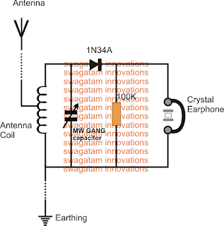
Circuit Description
Once the above mentioned antenna and the earthing is correctly set up, its time to connect the simple crystal radio circuit with these parameters.
Referring to the figure above, we see that the circuit hardly comprises any serious parts, it uses one antenna coil made by winding many turns of thin copper wire over a plastic bobbin with three wire ends terminating outwards, wherein the mid tap is used for the antenna connection.
The resonant tank circuit is formed by connecting a trimmer parallel to the antenna coil ends, this trimmer could be any MW GANG capacitor, again the same could be salvaged from any old radio set.
The radio signals are picked and resonated to the peak level through this tank circuit network, however in order to detect and demodulate the sound from the signals carrier waves we need another stage for this function.
An ordinary germanium diode is what we need to carry out the detection work and it does this quite effectively. Even our very familiar silicon 1N4148 could be tried for the job but only in case you are unable to procure the regular OA91 or the IN34A type of devices. And this part is the only active component involved in the whole circuit for reproducing the original sound from the captured signals, thats amazing.
How to Wind the Antenna Coil:
The antenna coil is an air cored winding, its built with the following simple steps:
You will need a 1 or 1.5 inch diameter, and 4 inches long plastic pipe for the bobbin.
Over this pipe wind some 65 turns of any thin super enameled copper wire or any thin insulated flexible wire such as a 7/36 multi strand insulated wire.
Make sure to pull out a center tap at around 18th turn of the winding, or some other number tap can also experimented with for trying preferred customized receptions.
Thats all, the antenna coil is ready and may be used for the above explained simple crystal radio circuit.
If you have any questions or doubts, dont hesitate to put it forth through comments below
The only downside of this radio concept is the requirement of a very long antenna and a deep earthing, therefore this unit is not something which you can carry in your pocket, nevertheless the extreme simplicity and the no power operation feature make this circuit an amazing device.
The main components involved with this simple crystal radio set circuit are an ordinary antenna coil, a detector diode, an optional resistor, and a crystal earphone. The detector diode could be any regular germanium diode such as OA91 or 1N34A etc.
A crystal earphone is recommended here, due to its high impedance property, which makes it a voltage sensitive device rather than a current sensitive device.
Meaning the earphone would be able to transform even the weakest of voltage frequencies regardless of the current (mA) magnitude, enabling hearing of even the feeblest of the radio signals. This is crucial since no external power is being used for the amplification.
Typically a crystal earphone with a range of 2K ohms should be just good enough value for our crystal radio application.
To check the efficiency level of a crystal earphone, you could probably do a few simple but very interesting tests with it.
The first test could be performed by simply scratching the end terminals of its wires with each other, this should produce faint clicking sound in the earphone, another test can be tried by firmly holding the stripped ends of its wires and standing near your home mains line....this should enable you to hear a reasonably strong humming sound in the earphone. These tests might be enough to convince you regarding the high level of sensitivity that these units may be specified with.
This high sensitivity of the crystal earphone along with the resonant tuning of the radios LC tank circuit stage, together ensures a sound level thats loud enough to be clearly heard without using any form of external power supply.
With no external power, the weak electrical pulses of the radio signal is itself processed and used by the crystal circuit and the crystal earphone and is made efficiently audible in our ears.
This radio can be used for hearing local stations at around 50kms range during daytime and from over 100 of miles away at night when the surrounding noise is much reduced compared to the daytime commotion.
The key element that helps the crystal set to grab even the minutest of radio reception is the length of the antenna used, it should be preferably a 30to 40 meter long flexible wire suitably tied and hung at some elevation such as a tree branch etc.
The antenna will be capable of capturing quite many radio stations including the night time DX stations, due to the favorable ionosphere transition after the sun goes down.
The second crucial element of the design is the "earthing" or the ground quality, which should not be ignored otherwise the radio could simply refuse to provide the intended results.
A perfect ground can be achieved by inserting a steel rod deep into a 5 feet hole dug on earth which should be first adequately watered to make it soft and then a bag of salt thrown into it to make things sufficiently conductive, and for creating an efficient grounding for the circuit.
Another easy method for achieving the earthing is by using the tap or the metallic plumbing line of your bathroom which also would act as a very good earthing for the circuit.
Circuit Description
Once the above mentioned antenna and the earthing is correctly set up, its time to connect the simple crystal radio circuit with these parameters.
Referring to the figure above, we see that the circuit hardly comprises any serious parts, it uses one antenna coil made by winding many turns of thin copper wire over a plastic bobbin with three wire ends terminating outwards, wherein the mid tap is used for the antenna connection.
The resonant tank circuit is formed by connecting a trimmer parallel to the antenna coil ends, this trimmer could be any MW GANG capacitor, again the same could be salvaged from any old radio set.
The radio signals are picked and resonated to the peak level through this tank circuit network, however in order to detect and demodulate the sound from the signals carrier waves we need another stage for this function.
An ordinary germanium diode is what we need to carry out the detection work and it does this quite effectively. Even our very familiar silicon 1N4148 could be tried for the job but only in case you are unable to procure the regular OA91 or the IN34A type of devices. And this part is the only active component involved in the whole circuit for reproducing the original sound from the captured signals, thats amazing.
How to Wind the Antenna Coil:
The antenna coil is an air cored winding, its built with the following simple steps:
You will need a 1 or 1.5 inch diameter, and 4 inches long plastic pipe for the bobbin.
Over this pipe wind some 65 turns of any thin super enameled copper wire or any thin insulated flexible wire such as a 7/36 multi strand insulated wire.
Make sure to pull out a center tap at around 18th turn of the winding, or some other number tap can also experimented with for trying preferred customized receptions.
Thats all, the antenna coil is ready and may be used for the above explained simple crystal radio circuit.
If you have any questions or doubts, dont hesitate to put it forth through comments below
Available link for download
Sunday, August 21, 2016
Simple Touch Sensor Switch Circuit
Simple Touch Sensor Switch Circuit
A simple touch sensor switch circuit can be built using a single IC 4017 and a few other passive components, the procedure is explained in the following article.
Referring to the below given circuit diagram for the proposed simple touch sensor switch, we can see that the entire design is built around the IC 4017 which is a 10 step johnsons decade counter divider chip.

The IC basically consists of 10 outputs, starting from its pin#3 and randomly ending at pin#11, constituting 10 outputs which are designed to produce a sequencing or shifting high logics across these output pins in response to every single positive pulse applied at its pin#14.
The sequencing does not need to finish at the last pin#11, rather could be assigned to stop at any desired intermediate pinout, and revert to the first pin#3 to initiate the cycle afresh.
This is simply done by connecting the end sequence pinout with the reset pin#15 of the IC. This makes sure that whenever the sequence reaches this pinout, the cycle stops here and reverts to pin#3 which is the initial pinout for enabling a repeat cycling of the sequence in the same order.
For example in our design pin#4 which is the third pinout in the sequence can be seen attached to pin#15 of the IC, implies that as the sequence jumps from pin#3 to the next pin#2, and then to pin#4 it instantly reverts or flips back to pin#3 to enable the cycle again.
This cycling is induced by touching the indicated touch plate which causes a positive pulse to appear at pin#14 of the IC each time its touched.
Lets assume at power switch ON the high logic is at pin#3, this pin is not connected anywhere and is unused, while pin#2 can be seen connected with the relay driver stage, therefore at this moment the relay stays switched OFF.
As soon as the touch plate is tapped, the positive pulse at pin#14 of the IC toggles the output sequence which now jumps from pin#3 to pin#2 enabling the relay to switch ON.
The position is held fixed at this point, with the relay in the switched ON position and the connected load activated.
However as soon as the touch plate is touched again, the sequence is forced to jump from pin#2 to pin#4, which in turn prompts the IC to revert the logic back to pin#3, shutting of the relay and the load and enabling the IC back to its standby condition.
Referring to the below given circuit diagram for the proposed simple touch sensor switch, we can see that the entire design is built around the IC 4017 which is a 10 step johnsons decade counter divider chip.
The IC basically consists of 10 outputs, starting from its pin#3 and randomly ending at pin#11, constituting 10 outputs which are designed to produce a sequencing or shifting high logics across these output pins in response to every single positive pulse applied at its pin#14.
The sequencing does not need to finish at the last pin#11, rather could be assigned to stop at any desired intermediate pinout, and revert to the first pin#3 to initiate the cycle afresh.
This is simply done by connecting the end sequence pinout with the reset pin#15 of the IC. This makes sure that whenever the sequence reaches this pinout, the cycle stops here and reverts to pin#3 which is the initial pinout for enabling a repeat cycling of the sequence in the same order.
For example in our design pin#4 which is the third pinout in the sequence can be seen attached to pin#15 of the IC, implies that as the sequence jumps from pin#3 to the next pin#2, and then to pin#4 it instantly reverts or flips back to pin#3 to enable the cycle again.
This cycling is induced by touching the indicated touch plate which causes a positive pulse to appear at pin#14 of the IC each time its touched.
Lets assume at power switch ON the high logic is at pin#3, this pin is not connected anywhere and is unused, while pin#2 can be seen connected with the relay driver stage, therefore at this moment the relay stays switched OFF.
As soon as the touch plate is tapped, the positive pulse at pin#14 of the IC toggles the output sequence which now jumps from pin#3 to pin#2 enabling the relay to switch ON.
The position is held fixed at this point, with the relay in the switched ON position and the connected load activated.
However as soon as the touch plate is touched again, the sequence is forced to jump from pin#2 to pin#4, which in turn prompts the IC to revert the logic back to pin#3, shutting of the relay and the load and enabling the IC back to its standby condition.
Available link for download
Subscribe to:
Posts (Atom)