Showing posts with label inverter. Show all posts
Showing posts with label inverter. Show all posts
Tuesday, November 8, 2016
Synchronized 4kva Stackable Inverter Circuit Part 2
Synchronized 4kva Stackable Inverter Circuit Part 2
In the previous part of this article we learned the main section of the 4kva synchronized stackable inverter circuit which explained the synchronization details of the design. In this article we study how to make the design a sinewave equivalent and also ensure correct synchronization of the PWMs across the involved inverters.
Synchronizing Sine Wave PWM across the Inverters
A simple RMS matched PWM equivalent sinewave waveform generator can be made by using an IC 555 and IC 4060, as shown in the following figure.This design can be then used for enabling the inverters to produce a sinewave equivalent waveform at their outputs, and across the connected mains line.
Each of these PWM processors would be required for each of the stackable inverter modules individually.

The different stages involved in the above PWM geneartor circuit can be understood with the help of the following point:
The IC 555 is configured as the basic PWM generator circuit. To be able to generate an adjustable PWM equivalent pulses at the desired RMS the IC requires fast triangle waves at its pin7 and a reference potential at its pin5 which determines the PWM level at its output pin#3
For generating the triangle waves, the IC 555 requires square waves at its pin#2, which is acquired from the IC 4060 oscillator chip.
The IC 4060 determines the frequency of the PWM, or simply the number of "pillars" in each of the AC half cycles.
The IC 4060 is mainly employed for multiplying the sample low frequency content from the inverter output into a relatively high frequency from its pin#7. The sample frequency basically makes sure that the PWM chopping is equal and synchronized for all the invetrer modules. This is main reason why the IC 4060 is included otherwise another IC 555 could have easy done the job, instead.
The reference potential at pin#5 of IC 555 is acquired from an opamp voltage follower shown at extreme left of the circuit.
As the name suggests this opamp delivers exactly the same magnitude of voltage at its pin#6 which appears at its pin#3....however the pin#6 replication of its pin#3 is nicely buffered, and therefore is richer than its pin3 quality, and thats the exact reason of including this stage in the design.
The 10 k preset associated at pin3 of this IC is used for adjusting the RMS level which ultimately fine tunes the the IC 555 output PWMs to the desired RMS level.
This RMS is then applied to the bases of the power devices in order to force them to work at the specified PWM RMS levels, which in turn causes the output AC to acquire a pure sinewave like attribute through a correct RMS level. This may be further enhanced by employing an LC filter across the output winding of the all the transformers.
The next and the final part of this 4kva stackable synchronized inverter circuit details the automatic load correction feature for enabling the inverters to deliver and maintain the correct amount wattage across the output power mains line in accordance with the varying loads switching.
Available link for download
Friday, November 4, 2016
Synchronized 4kva Stackable Inverter Circuit Part 3
Synchronized 4kva Stackable Inverter Circuit Part 3
We have so far covered the two main requirements for the proposed synchronized 4kva stackable inverter circuit, which includes synchronization of frequency, phase and PWM across the inverters so that failing of any of the inverters had no effect on the rest in terms of the above parameters.
In this article we will try to figure out the automatic load correction feature which may enable the switching ON or OFF of the inverters sequentially in response to the varying load conditions across the output mains line.
A simple quad comparator using LM324 IC can be used for implementing an automatic sequential load correction as indicated in the following diagram:

In the figure above we can see four opamps from the IC LM324 configured as four separate comparators with their non-inverting inputs rigged with individual presets,while their inverting inputs all referenced with a fixed zener voltage.
The relevant presets are simply adjusted such that the opamps produce high outputs in a sequential a soon as the mains voltage goes above the intended threshold..... and vice versa.
When this happens the relevant transistors switch in accordance with the opamp activation.
The collectors of the respective BJTs are connected with the pin#3 of the voltage follower opamp IC 741 which is employed in the PWM controller stage, and this forces the opamp output to go low or zero, which in turn causes a zero voltage to appear at pin#5 of the PWM IC 555 (as discussed in Part 2).
With pin#5 of the IC 555 is applied with this zero logic, forces the PWMs to become narrowest or at the minimum value, which causes the output of that particular inverter to almost shut down.
The above actions make an attempt to stabilize the output to an earlier normal condition which again forces the PWM to get wider and this tug-of-war or a constant switching of the opamps cintinues consistently keeping the output as stable as possible, in response to the variations of the attached loads.
With this automatic load correction implemented within the proposed 4kva stackable inverter circuit almost makes the design complete with all the features requested by the user in Part 1 of the article.
In this article we will try to figure out the automatic load correction feature which may enable the switching ON or OFF of the inverters sequentially in response to the varying load conditions across the output mains line.
A simple quad comparator using LM324 IC can be used for implementing an automatic sequential load correction as indicated in the following diagram:
In the figure above we can see four opamps from the IC LM324 configured as four separate comparators with their non-inverting inputs rigged with individual presets,while their inverting inputs all referenced with a fixed zener voltage.
The relevant presets are simply adjusted such that the opamps produce high outputs in a sequential a soon as the mains voltage goes above the intended threshold..... and vice versa.
When this happens the relevant transistors switch in accordance with the opamp activation.
The collectors of the respective BJTs are connected with the pin#3 of the voltage follower opamp IC 741 which is employed in the PWM controller stage, and this forces the opamp output to go low or zero, which in turn causes a zero voltage to appear at pin#5 of the PWM IC 555 (as discussed in Part 2).
With pin#5 of the IC 555 is applied with this zero logic, forces the PWMs to become narrowest or at the minimum value, which causes the output of that particular inverter to almost shut down.
The above actions make an attempt to stabilize the output to an earlier normal condition which again forces the PWM to get wider and this tug-of-war or a constant switching of the opamps cintinues consistently keeping the output as stable as possible, in response to the variations of the attached loads.
With this automatic load correction implemented within the proposed 4kva stackable inverter circuit almost makes the design complete with all the features requested by the user in Part 1 of the article.
Available link for download
Thursday, October 13, 2016
PWM Sinewave 5kva Inverter Circuit
PWM Sinewave 5kva Inverter Circuit
The post discusses a 5kva PWM sinewave inverter circuit using compact ferrite core transformer. The idea was requested by Mr. Javeed.
The Request
dear sir, would you please modify its output with PWM source and facilitate to make use such an inexpensive and economical design to World wide needy people like us? Hope You will consider my request.Thanking you.Your affectionate reader.
Javeed Ahmed
The Design
In one of my previous post I introduced a ferrite core based 5kva inverter circuit, but since it is a square wave inverter it cannot be used with the various electronic equipment, and therefore its application may be restricted to only with the resistive loads.
However, the same design could be converted into a PWM equivalent sine wave inverter by injecting a PWM feed into the low side mosfets as shown in the following diagram:
 The SD pin is mistakenly shown connected with Ct, please be sure to keep it unused or blank.
As we can see in the above PWM based 5kva Inverter circuit, the design is exactly similar to our earlier original 5kva inverter circuit, except the indicated PWM buffer feed stage with the low side mosfets of the H-bridge driver stage.
The PWM feed insertion could be acquired through any standard PWM generator circuit using IC 555 or by using transistorized astable multivibrator.
For more accurate PWM replication, one can also opt for a Bubba oscilator PWM generator for sourcing the PWM with the above shown 5kva sinewave inverter design.
The construction procedures for the above design is not different to the original design, the only difference being the integration of the BC547/BC557 BJT buffer stages with the low side mosfets of the full bridge IC stage and the PWM feed into it.
UPDATE:
A careful inspection of the PWM section of the above 5kva sinewave inverter circuit shows that it may not be correctly configured. The correct method of implementing this can be witnessed in the following updated diagram:

The Request
dear sir, would you please modify its output with PWM source and facilitate to make use such an inexpensive and economical design to World wide needy people like us? Hope You will consider my request.Thanking you.Your affectionate reader.
Javeed Ahmed
The Design
In one of my previous post I introduced a ferrite core based 5kva inverter circuit, but since it is a square wave inverter it cannot be used with the various electronic equipment, and therefore its application may be restricted to only with the resistive loads.
However, the same design could be converted into a PWM equivalent sine wave inverter by injecting a PWM feed into the low side mosfets as shown in the following diagram:
As we can see in the above PWM based 5kva Inverter circuit, the design is exactly similar to our earlier original 5kva inverter circuit, except the indicated PWM buffer feed stage with the low side mosfets of the H-bridge driver stage.
The PWM feed insertion could be acquired through any standard PWM generator circuit using IC 555 or by using transistorized astable multivibrator.
For more accurate PWM replication, one can also opt for a Bubba oscilator PWM generator for sourcing the PWM with the above shown 5kva sinewave inverter design.
The construction procedures for the above design is not different to the original design, the only difference being the integration of the BC547/BC557 BJT buffer stages with the low side mosfets of the full bridge IC stage and the PWM feed into it.
UPDATE:
A careful inspection of the PWM section of the above 5kva sinewave inverter circuit shows that it may not be correctly configured. The correct method of implementing this can be witnessed in the following updated diagram:
Available link for download
Thursday, September 29, 2016
Simple 5 Level Cascaded Sine Wave Inverter Circuit
Simple 5 Level Cascaded Sine Wave Inverter Circuit
In this article we learn how to make a multilevel (5 level) cascaded inverter circuit using a very simple concept developed by me. Lets learn more regarding the details.
In this website so far I have developed, designed and introduced many sine wave inverter circuits using straightforward concepts and ordinary components such as IC 555, which happen to be more result oriented instead of being complex and full of theoretical jumbles.
I have explained how simply a high power audio amplifier can be converted into a pure sine wave inverter, and I have also covered comprehensively regarding sine wave inveters using SPWM concept as given below:
Pure Sine Wave Inverter Circuit Using IC 4047
300 Watts PWM Controlled, Pure Sine Wave Inverter Circuit ...
Simple Pure Sine Wave Inverter Circuit - 500 Watt Pure Sine
Make this IC 556 Pure Sine Wave Inverter circuit
Sine Wave Inverter Circuit using Bubba Oscillator
We have also learned through this website regarding how to convert any square inverter into a pure sine wave inverter design.
Assessing the above sine wave inverter circuits using sine equivalent PWMs, we understand that the waveform of SPWMs do not directly match or coincide with an actual sinusoidal waveform, rather these execute the sine wave effect or results by interpreting the RMS value of the actual sine wave AC.
Although SPWM can be considered an effective way of replicating and implementing a reasonably pure sine wave, the fact that it does not simulate or coincide with a real sine wave makes the concept a little unsophisticated, especially if compared to a 5 Level cascaded sine wave inverter concept.
We can compare and analyze the two types of sine wave simulation concepts by referring to the following images:

We can clearly see that the 5 level cascaded concept produces a more obvious and effective simulation of a real sine wave than the SPWM concept which relies solely on matching the RMS value with the original sine wave magnitude.
Designing a conventional 5 Level Cascaded sine wave Inverter can be quite complex, but the concept which is explained here makes the implementation easier and employs ordinary components.
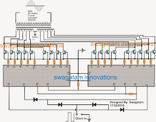
Referring to the image above, we can see how simply the 5 level cascaded inverter concept can be practically implemented using just a muti-tap transformer, a couple of 4017 ICs and 18 power BJTs, which could be easily replaced with mosfets if required.
Here a couple of 4017 ICs which are Johnsons 10 stage counter divider chips, are cascaded to produce a sequentially running or chasing logic highs across the shown pinouts of the ICs.
These sequentially running logic are used for triggering the connected power BJTs in the same sequence which in turn switch the transformer winding in an order which causes the transformer to produce a cascaded kind of sine equivalent waveform.
The transformer forms the heart of the circuit and employs a specially wounded primary with 11 taps. These taps are simply extracted uniformly from a single long calculated winding.
The BJTs associated with one of the ICs switch one of the halves of the transformer through 5 taps enabling the generation of 5 level steps, constituting one half cycle of the AC waveform, while the BJTs associated with the other ICs does the identical function to shape up the lower half AC cycle in the form of 5 level cascaded waveform.
The ICs are run by clock signals applied to the indicated position in the circuit, which could be acquired from any standard 555 IC astable circuit.
The first 5 sets of the BJTs build up the 5 levels of the waveform, the remaining 4 BJTs switch the same in reverse order to complete the cascaded waveform having a total of 9 skyscrapers.
These skyscrapers are formed by producing an ascending and descending voltage levels by the switching of the corresponding winding of the transformer which are rated at the relevant voltage levels
For example, winding #1 could be rated at 150V with respect to the center tap, the winding #2 at 200V, winding #3 at 230V, winding #4 at 270V and winding #5 at 330V, so when these are switched sequentially by the set of the shown 5 BJTs, we get the first 5 levels of the waveform, next when these winding are switched in reverse by the following 4 BJTs it creates the descending 4 level waveforms, thus completing the upper half cycle of the 220V AC.
The same is repeated by the other 9 BJTs associated with the other 4017 IC giving rise to the lower half of the 5 level cascaded AC, which completes one complete AC waveform of the required 220V AC output.
Transformer Details:

As may be witnessed in the above diagram, the transformer is an ordinary iron core type, made by winding the primary and the secondary with turns corresponding to the indicated voltage taps.
When connected with the corresponding BJTs these winding can be expected to induce a 5 level or a total of 9 level of cascaded waveform wherein the first 36V winding would correspond and induce a 150V, the 27V would induce an equivalent of 200V, while the 20V, 27V, 36V would be responsible of producing 230V, 270V and 330V across the secondary winding in the proposed cascaded format.
The set of taps on the lower side of the primary would carry out the switching to complete 4 ascending levels of the waveform.
An identical procedure would be repeated by the 9 BJTs associated with the complementary 4017 IC for building the negative half cycle of the AC...the negative is rendered due to the opposite orientation of the transformer winding with respect to the center tap.
Update:
Complete circuit diagram of the discussed multi-level cascaded sinewave inverter circuit
 The 1M pot associated with the 555 circuit will need to be adjusted for setting up a 50Hz or a 60Hz frequency for the inverter as per the country specs of the user.
Parts List
All unspecified resistors are 10k, 1/4 watt
All diodes are 1N4148
All BJTs are TIP142
ICs are 4017
In this website so far I have developed, designed and introduced many sine wave inverter circuits using straightforward concepts and ordinary components such as IC 555, which happen to be more result oriented instead of being complex and full of theoretical jumbles.
I have explained how simply a high power audio amplifier can be converted into a pure sine wave inverter, and I have also covered comprehensively regarding sine wave inveters using SPWM concept as given below:
Pure Sine Wave Inverter Circuit Using IC 4047
300 Watts PWM Controlled, Pure Sine Wave Inverter Circuit ...
Simple Pure Sine Wave Inverter Circuit - 500 Watt Pure Sine
Make this IC 556 Pure Sine Wave Inverter circuit
Sine Wave Inverter Circuit using Bubba Oscillator
We have also learned through this website regarding how to convert any square inverter into a pure sine wave inverter design.
Assessing the above sine wave inverter circuits using sine equivalent PWMs, we understand that the waveform of SPWMs do not directly match or coincide with an actual sinusoidal waveform, rather these execute the sine wave effect or results by interpreting the RMS value of the actual sine wave AC.
Although SPWM can be considered an effective way of replicating and implementing a reasonably pure sine wave, the fact that it does not simulate or coincide with a real sine wave makes the concept a little unsophisticated, especially if compared to a 5 Level cascaded sine wave inverter concept.
We can compare and analyze the two types of sine wave simulation concepts by referring to the following images:
We can clearly see that the 5 level cascaded concept produces a more obvious and effective simulation of a real sine wave than the SPWM concept which relies solely on matching the RMS value with the original sine wave magnitude.
Designing a conventional 5 Level Cascaded sine wave Inverter can be quite complex, but the concept which is explained here makes the implementation easier and employs ordinary components.
Referring to the image above, we can see how simply the 5 level cascaded inverter concept can be practically implemented using just a muti-tap transformer, a couple of 4017 ICs and 18 power BJTs, which could be easily replaced with mosfets if required.
Here a couple of 4017 ICs which are Johnsons 10 stage counter divider chips, are cascaded to produce a sequentially running or chasing logic highs across the shown pinouts of the ICs.
These sequentially running logic are used for triggering the connected power BJTs in the same sequence which in turn switch the transformer winding in an order which causes the transformer to produce a cascaded kind of sine equivalent waveform.
The transformer forms the heart of the circuit and employs a specially wounded primary with 11 taps. These taps are simply extracted uniformly from a single long calculated winding.
The BJTs associated with one of the ICs switch one of the halves of the transformer through 5 taps enabling the generation of 5 level steps, constituting one half cycle of the AC waveform, while the BJTs associated with the other ICs does the identical function to shape up the lower half AC cycle in the form of 5 level cascaded waveform.
The ICs are run by clock signals applied to the indicated position in the circuit, which could be acquired from any standard 555 IC astable circuit.
The first 5 sets of the BJTs build up the 5 levels of the waveform, the remaining 4 BJTs switch the same in reverse order to complete the cascaded waveform having a total of 9 skyscrapers.
These skyscrapers are formed by producing an ascending and descending voltage levels by the switching of the corresponding winding of the transformer which are rated at the relevant voltage levels
For example, winding #1 could be rated at 150V with respect to the center tap, the winding #2 at 200V, winding #3 at 230V, winding #4 at 270V and winding #5 at 330V, so when these are switched sequentially by the set of the shown 5 BJTs, we get the first 5 levels of the waveform, next when these winding are switched in reverse by the following 4 BJTs it creates the descending 4 level waveforms, thus completing the upper half cycle of the 220V AC.
The same is repeated by the other 9 BJTs associated with the other 4017 IC giving rise to the lower half of the 5 level cascaded AC, which completes one complete AC waveform of the required 220V AC output.
Transformer Details:
As may be witnessed in the above diagram, the transformer is an ordinary iron core type, made by winding the primary and the secondary with turns corresponding to the indicated voltage taps.
When connected with the corresponding BJTs these winding can be expected to induce a 5 level or a total of 9 level of cascaded waveform wherein the first 36V winding would correspond and induce a 150V, the 27V would induce an equivalent of 200V, while the 20V, 27V, 36V would be responsible of producing 230V, 270V and 330V across the secondary winding in the proposed cascaded format.
The set of taps on the lower side of the primary would carry out the switching to complete 4 ascending levels of the waveform.
An identical procedure would be repeated by the 9 BJTs associated with the complementary 4017 IC for building the negative half cycle of the AC...the negative is rendered due to the opposite orientation of the transformer winding with respect to the center tap.
Update:
Complete circuit diagram of the discussed multi-level cascaded sinewave inverter circuit
Parts List
All unspecified resistors are 10k, 1/4 watt
All diodes are 1N4148
All BJTs are TIP142
ICs are 4017
Available link for download
Friday, September 9, 2016
Solar Inverter Circuit for 1 5 Ton AC
Solar Inverter Circuit for 1 5 Ton AC
Here we learn how to build a solar inverter circuit for a 1.5 ton air conditioner (AC) for powering the AC during daytime directly from solar panels without depending on grid power. The idea was requested by Mr. Subhashish.
A 1.5 ton air conditioner is equivalent to an approximately 1.5 x 1200 = 1800 watts load which is quite huge. In order to fulfill this formidable load the solar panel spec needs to be equally robust and rated with sufficiently high voltage and current specs.
Solar panels are generally rated at lower currents compared to their voltage ratings, which in turn heavily depend on the sunlight conditions. These parameters make these devices quite inefficient with their operations and managing their power optimally becomes a challenging task for the end user.
To tackle this, sophisticated controllers such MPPT solar charge controller are designed and can be effectively implemented for acquiring the maximum from solar panels, yet still calculating a solar panel for higher loads is never an easy job for any concerned technician.
A 1.5 ton air conditioner will probably require a 2000 watt solar panel, this value will need to be ascertained with practical experimentation.
The air conditioner will be normally a 220V or 120V operated device, and therefore the panel will also need to be rated at this voltage ideally in order to produce the most efficient results without using complex controller circuits.
This can be implemented by using 60V panels in series, which means 5 such panels would need to be connected series, with each pane rated at 2000/300 = 6.66 amps, or practically a 10amp value would be just enough.
This voltage will be a pure DC, therefore this will need to be converted to AC for operating the air conditioner.
The conversion from DC to AC can be simply done by a using a full bridge inverter circuit as shown below:

Circuit Description
The IC IRS2453 enables the making of an efficient full bridge inverter circuit extremely easy. As can be seen the output of the IC just needs 4 N channel mosfets to be integrated for implementing a full bridge inverter actions.
The IC has a built-in oscillator, so no external oscillator stage is required for initiating the shown IRS2453 IC circuit. The Rt, Ct network associated with the IC determines the operating frequency of the inverter, and is supposed to be set at 50Hz or 60Hz depending on whether the operating voltage of the air conditioner is 220V or 120V respectively.
The IC 555 shown the left of the design is employed for generating a sine wave equivalent PWM feed for the full bridge inverter output.
The controlled PWM from the IC 555 is fed to the gates of the low side mosfets via the buffer transistor stage made through the BC547/BC557 pairs.
The above PWM feed helps the load to operate with an optimized RMS and alternating current which can be expected to be a close equivalent of the sinusoidal mains AC waveform.
The two pots associated with the IC 555 needs to be correctly adjusted until the required RMS and waveform is determined for the air conditioner.
The 300V from the solar panel can be seen connected with the high side mosfet drains, which is stepped down to 15V through the indicated 33K, and 15V zener diode for providing a safe Vcc operating voltage for the two ICs.
Once the above procedures are implemented and appropriately set, the proposed 1.5 ton air conditioner can be effectively run throughout the day using only solar panels, without the need of any grid or utility power inputs.
A 1.5 ton air conditioner is equivalent to an approximately 1.5 x 1200 = 1800 watts load which is quite huge. In order to fulfill this formidable load the solar panel spec needs to be equally robust and rated with sufficiently high voltage and current specs.
Solar panels are generally rated at lower currents compared to their voltage ratings, which in turn heavily depend on the sunlight conditions. These parameters make these devices quite inefficient with their operations and managing their power optimally becomes a challenging task for the end user.
To tackle this, sophisticated controllers such MPPT solar charge controller are designed and can be effectively implemented for acquiring the maximum from solar panels, yet still calculating a solar panel for higher loads is never an easy job for any concerned technician.
A 1.5 ton air conditioner will probably require a 2000 watt solar panel, this value will need to be ascertained with practical experimentation.
The air conditioner will be normally a 220V or 120V operated device, and therefore the panel will also need to be rated at this voltage ideally in order to produce the most efficient results without using complex controller circuits.
This can be implemented by using 60V panels in series, which means 5 such panels would need to be connected series, with each pane rated at 2000/300 = 6.66 amps, or practically a 10amp value would be just enough.
This voltage will be a pure DC, therefore this will need to be converted to AC for operating the air conditioner.
The conversion from DC to AC can be simply done by a using a full bridge inverter circuit as shown below:
Circuit Description
The IC IRS2453 enables the making of an efficient full bridge inverter circuit extremely easy. As can be seen the output of the IC just needs 4 N channel mosfets to be integrated for implementing a full bridge inverter actions.
The IC has a built-in oscillator, so no external oscillator stage is required for initiating the shown IRS2453 IC circuit. The Rt, Ct network associated with the IC determines the operating frequency of the inverter, and is supposed to be set at 50Hz or 60Hz depending on whether the operating voltage of the air conditioner is 220V or 120V respectively.
The IC 555 shown the left of the design is employed for generating a sine wave equivalent PWM feed for the full bridge inverter output.
The controlled PWM from the IC 555 is fed to the gates of the low side mosfets via the buffer transistor stage made through the BC547/BC557 pairs.
The above PWM feed helps the load to operate with an optimized RMS and alternating current which can be expected to be a close equivalent of the sinusoidal mains AC waveform.
The two pots associated with the IC 555 needs to be correctly adjusted until the required RMS and waveform is determined for the air conditioner.
The 300V from the solar panel can be seen connected with the high side mosfet drains, which is stepped down to 15V through the indicated 33K, and 15V zener diode for providing a safe Vcc operating voltage for the two ICs.
Once the above procedures are implemented and appropriately set, the proposed 1.5 ton air conditioner can be effectively run throughout the day using only solar panels, without the need of any grid or utility power inputs.
Available link for download
Thursday, September 8, 2016
Synchronized 4kva Stackable Inverter Circuit Part 1
Synchronized 4kva Stackable Inverter Circuit Part 1
This first part of the proposed 4kva synchronized stackable inverter circuit discusses how to implement the crucial automatic synchronization across the 4 inverters with regards to frequency, phase and voltage to keep the inverters running independent of each other yet achieving an output thats on par with each other.
The idea was requested by Mr. David. The following email conversation between him and me details the main specs of the proposed Synchronized 4kva Stackable Inverter Circuit.
Email#1
Hi Swagatam,
Firstly I wanted to say thank you for your contribution to the world at large, the information and most importantly your willingness to share your knowledge to help other people in my opinion is invaluable for many reasons.
I would like to enhance some of the circuits you have shared to suit my own purposes, unfortunately whilst I understand what is going on in the circuits I lack the creativity and knowledge to make the amendments myself.
I can generally follow circuits if they are small and I can see where they join/connect into bigger schematics. If I may I would like to try to explain what I would like to achieve, though I am under no illusion that you are a very busy person and would not like take up your precious time unnecessarily.
The final goal would be that I would like to build ( assemble the components ) of a multi-source renewable energy micro grid, using Solar PV, Windmills, and bio diesel generators.
The first step is the PV solar inverter enhancements. I would like to use your 48 volt pure sine wave inverter circuit capable of maintaining a constant 2kW 230V output, it must be capable of delivering at least 3 times this output for a very short duration.
The key modification that I want to achieve it to create a number of these inverters units to work in parallel and connected to an AC bus bar. I would like each inverter to independently and constantly sample the AC bus bar for frequency, voltage and current (load).
I will call these inverters slave units. The idea being the invert modules will be “plug and play”.
The inverter once connected to the AC bus bar would constantly sample/measure the frequency on the AC bus bar and use this information to drive the input of a 4047 IC such that its clock output can be advanced or retarded until it exactly clones the frequency on the AC bus bar once the two wave forms are synchronized the inverter will close a contactor or relay which connects the invert output stage to the AC bus bar.
In the event that the frequency on the bar or the voltage moves outside of a pre-determined tolerance the inverter module should open the relay or contactor on the output stage effectively disconnecting the inverter output stage from the AC bar to protect its self.
Additionally once connected to the AC bus bar the slave units would go to sleep or at least the output stage of the inverter would sleep while the load on the bar is less than the sum of all of the slave inverters. Imagine if you will there are 3 slave inverters attached to the AC bus bar, however the load on the bar is only 1.8kW then the other two slaves would go to sleep.
The reciprocal would also be true that if the load on the bar jumped to say 3kW one of the sleeping inverts would instantly wake (already be in sync) to supply the additionally required energy.
I imagine some large capacitors on each of the output stage would supply the energy required whilst the inverter has the very short moment whilst it wakes up. It would be preferable (only in my opinion) not to directly connect each inverter to each other but rather that they be independently autonomous.
I want to try to avoid micro controllers or the units error or fault checking each other or the units having ‘address’s’ on the system. In my mind’s eye I imagine that the first connected device on the AC bus bar would be a very stable reference inverter that is constantly connected.
This reference inverter would provide the frequency and voltage that the other slave units would use to generate their own respective outputs.
Unfortunately I can’t get my head around how you could prevent a feedback loop where the slave units would each potentially end up becoming the reference unit. Beyond the scope of this email I have some small generators I would like to connect to the AC bus bar synchronizing to the reference inverter to supply energy in the event that the load exceeds the DC max output capacity.
The overall premise is that the load presented to the AC bus bar would determine how many inverters and ultimately how many generators would either autonomously connect or disconnect to meet the demand as this would hopefully save energy or at least not waste energy.
The system being completely built of multiple modules would then be expandable/contractible as well as robust/resilient such that if anyone or perhaps two units were to fail the system would continue to function all be it at reduced capacity. I have attached a block diagram and excluded the battery charging for the time being.
I plan on charging the battery bank from the AC bus and rectifying down to 48V DC this way I can charge from the generators or the renewable energy sources, I do recognize that this is perhaps not as efficient as using DC mppt but I think what I lose in efficiency I gain in flexibility. I live a long way from town or the utility grid.
For reference there would be a minimum constant load on the AC bus bar of 2kW’s though the peak load could rise by as much as 30kW.
My plan is for the 1st 10 to 15kW to be provided by the solar PV panels and two 3kW (peak) windmills the windmills are wild AC rectified to DC and a 1000Ah 48 volt battery bank. (Which I would like to avoid draining/discharging beyond 30% of its capacity to ensure battery life) the remaining infrequent and very intermittent energy demand would be satisfied by my generators.
This infrequent and intermittent load comes from my workshop.
I have been thinking that it may be prudent to build a capacitor bank to handle or pick up the system slack of any inductive load start up currents such as the motor on my air compressor and table saw.
But I am not sure at this time if there is not a better/cheaper way. Your thoughts and comments would be greatly appreciated and valued I hope you have time to get back to me. Thank you for your time and attention in advance.
Kind Regards
David
Sent from my BlackBerry® wireless device
My Reply
Hi David,
I have read your requirement and have hopefully understood it correctly.
Out of the 4 inverters, only one would be having its own frequency
generator, while others would be running by extracting the frequency from
this main inverter output, and thus all would be in sync with each other
and with this master inverters specs.
Ill try to design it and hope it works as expected and as per your
mentioned specs, however the implementation will need to be done by an
expert who should be capable of understanding the concept and modify/tweak
it to perfection wherever it might be required....otherwise succeeding
with this reasonably complex design could become extremely difficult.
I can only present the basic concept and the schematic....rest will need
to be done by the engineers from your side.
It might take me some time to complete, this since I already have many
pending requests in the Queue...Ill inform you as son as its posted
Best Regards
Swag
Email#2
My Reply
Thanks David,
Basically you want the inverters to be in sync with each other in terms of
frequency and phase, and also each one having the ability to become the
master inverter and takeover the charge, in case the previous one fails
due to some reason. Right?
Ill try to fix this with whatever knowledge I have and some common sense
and not by employing complex ICs or configurations.
Warmest Regards
Swag
Email#3
The Design
As requested by Mr. David, the proposed 4kva stackable power inverter circuits need to be in the form of 4 separate inverter circuits, which can be stacked up appropriately in sync with each other for supplying the correct amount of self-regulating power to the connected loads, depending on how these loads are switched ON and OFF.
And in case the second inveter also fails, the third inverter takes the command and plays the role of the master inverter.
The basic design for fulfilling the mentioned criteria is shown in the following diagram:

This is in fact done by integrating the the "slave" inverters through an opamp/optocoupler stage as indicated in the above design.
Initially, the master inverter#1 is switched ON, which allows the opamp 741 stage to get powered and to initialize the frequency and phase tracking of the output voltage.
Once this is initiated, the subsequent inverters are all switched ON for adding power to the mains line.
As can be seen the opamp output is connected with the timing capacitor of all the slave inverters through an opto coupler which force the slave inverters to follow the frequency and the phase angle of the master inverter.
However the interesting thing here is the latching factor of the opamp with the instantaneous phase and frequency information. This happens since all the inverters are now delivering and running at the specified frequency and phase from the master inverter, which implies if in case any of the inverters fail including the master inverter, the opamp is able to quickly track and inject the instantaneous frequency/phase info and force the existing inverters to run with this specifications, and the inverter in turn are able to sustain the feedbacks to the opamp stage to make the transitions seamless and self optimizing.
Therefore hopefully the opamp stage takes care of the first challenge of keeping all the proposed stackable inverters perfectly synchronized through a LIVE tracking of the available mains specification.
In the next part of the article well learn the synchronized PWM sinewave stage, which is the next crucial feature of the above discussed design.
The idea was requested by Mr. David. The following email conversation between him and me details the main specs of the proposed Synchronized 4kva Stackable Inverter Circuit.
Email#1
Hi Swagatam,
Firstly I wanted to say thank you for your contribution to the world at large, the information and most importantly your willingness to share your knowledge to help other people in my opinion is invaluable for many reasons.
I would like to enhance some of the circuits you have shared to suit my own purposes, unfortunately whilst I understand what is going on in the circuits I lack the creativity and knowledge to make the amendments myself.
I can generally follow circuits if they are small and I can see where they join/connect into bigger schematics. If I may I would like to try to explain what I would like to achieve, though I am under no illusion that you are a very busy person and would not like take up your precious time unnecessarily.
The final goal would be that I would like to build ( assemble the components ) of a multi-source renewable energy micro grid, using Solar PV, Windmills, and bio diesel generators.
The first step is the PV solar inverter enhancements. I would like to use your 48 volt pure sine wave inverter circuit capable of maintaining a constant 2kW 230V output, it must be capable of delivering at least 3 times this output for a very short duration.
The key modification that I want to achieve it to create a number of these inverters units to work in parallel and connected to an AC bus bar. I would like each inverter to independently and constantly sample the AC bus bar for frequency, voltage and current (load).
I will call these inverters slave units. The idea being the invert modules will be “plug and play”.
The inverter once connected to the AC bus bar would constantly sample/measure the frequency on the AC bus bar and use this information to drive the input of a 4047 IC such that its clock output can be advanced or retarded until it exactly clones the frequency on the AC bus bar once the two wave forms are synchronized the inverter will close a contactor or relay which connects the invert output stage to the AC bus bar.
In the event that the frequency on the bar or the voltage moves outside of a pre-determined tolerance the inverter module should open the relay or contactor on the output stage effectively disconnecting the inverter output stage from the AC bar to protect its self.
Additionally once connected to the AC bus bar the slave units would go to sleep or at least the output stage of the inverter would sleep while the load on the bar is less than the sum of all of the slave inverters. Imagine if you will there are 3 slave inverters attached to the AC bus bar, however the load on the bar is only 1.8kW then the other two slaves would go to sleep.
The reciprocal would also be true that if the load on the bar jumped to say 3kW one of the sleeping inverts would instantly wake (already be in sync) to supply the additionally required energy.
I imagine some large capacitors on each of the output stage would supply the energy required whilst the inverter has the very short moment whilst it wakes up. It would be preferable (only in my opinion) not to directly connect each inverter to each other but rather that they be independently autonomous.
I want to try to avoid micro controllers or the units error or fault checking each other or the units having ‘address’s’ on the system. In my mind’s eye I imagine that the first connected device on the AC bus bar would be a very stable reference inverter that is constantly connected.
This reference inverter would provide the frequency and voltage that the other slave units would use to generate their own respective outputs.
Unfortunately I can’t get my head around how you could prevent a feedback loop where the slave units would each potentially end up becoming the reference unit. Beyond the scope of this email I have some small generators I would like to connect to the AC bus bar synchronizing to the reference inverter to supply energy in the event that the load exceeds the DC max output capacity.
The overall premise is that the load presented to the AC bus bar would determine how many inverters and ultimately how many generators would either autonomously connect or disconnect to meet the demand as this would hopefully save energy or at least not waste energy.
The system being completely built of multiple modules would then be expandable/contractible as well as robust/resilient such that if anyone or perhaps two units were to fail the system would continue to function all be it at reduced capacity. I have attached a block diagram and excluded the battery charging for the time being.
I plan on charging the battery bank from the AC bus and rectifying down to 48V DC this way I can charge from the generators or the renewable energy sources, I do recognize that this is perhaps not as efficient as using DC mppt but I think what I lose in efficiency I gain in flexibility. I live a long way from town or the utility grid.
For reference there would be a minimum constant load on the AC bus bar of 2kW’s though the peak load could rise by as much as 30kW.
My plan is for the 1st 10 to 15kW to be provided by the solar PV panels and two 3kW (peak) windmills the windmills are wild AC rectified to DC and a 1000Ah 48 volt battery bank. (Which I would like to avoid draining/discharging beyond 30% of its capacity to ensure battery life) the remaining infrequent and very intermittent energy demand would be satisfied by my generators.
This infrequent and intermittent load comes from my workshop.
I have been thinking that it may be prudent to build a capacitor bank to handle or pick up the system slack of any inductive load start up currents such as the motor on my air compressor and table saw.
But I am not sure at this time if there is not a better/cheaper way. Your thoughts and comments would be greatly appreciated and valued I hope you have time to get back to me. Thank you for your time and attention in advance.
Kind Regards
David
Sent from my BlackBerry® wireless device
My Reply
Hi David,
I have read your requirement and have hopefully understood it correctly.
Out of the 4 inverters, only one would be having its own frequency
generator, while others would be running by extracting the frequency from
this main inverter output, and thus all would be in sync with each other
and with this master inverters specs.
Ill try to design it and hope it works as expected and as per your
mentioned specs, however the implementation will need to be done by an
expert who should be capable of understanding the concept and modify/tweak
it to perfection wherever it might be required....otherwise succeeding
with this reasonably complex design could become extremely difficult.
I can only present the basic concept and the schematic....rest will need
to be done by the engineers from your side.
It might take me some time to complete, this since I already have many
pending requests in the Queue...Ill inform you as son as its posted
Best Regards
Swag
Email#2
Hi Swagatam,
Thank you so much for your very prompt response.
Thats not quite what I had in mind but certainly represents an alternative.
My thought was that each unit would have two frequency measurement sub circuits one that looks at the frequency on the AC bus bar and this unit is used to create the clock pulse for the inverter sine wave generator.
The other frequency measurement sub circuit would look at the output from the inverter sine wave generator.
There would be a comparison circuit perhaps using an opamp array that would feed back into the inverter sine wave generator clock pulse to advance the clock signal or retard the clock signal until the output from the sine wave generator exactly matched the sine wave on the AC Bar.
Once the frequency of the output stage of the inverter matched the frequency of the AC bus bar there would be an SSR that would close connecting the output stage of the inverter onto the AC bar preferably at the zero cross over point.
This way any one inverter module could fail and the system would carry on functioning. the purpose of the master inverter was that of all the inverter modules it would never go to sleep and would provide the initial AC bar frequency. however if it failed then the other units would not be affected as long as one was online
The slave units should shut down or start up as the load changes.
Your observation was correct I am not an "electronics" man I am a mechanical and electrical engineer :-) I work with big plant items like chillers and generators and compressors.
As this project progresss, and starts to become more tangible would you be wiling/open to accept a money gift? I dont have much but I could perhaps gift some money via paypal to help suport your website hosting costs.
Thankyou again.
I look forward to hearing from you.
namaste
David
My Reply
Thanks David,
Basically you want the inverters to be in sync with each other in terms of
frequency and phase, and also each one having the ability to become the
master inverter and takeover the charge, in case the previous one fails
due to some reason. Right?
Ill try to fix this with whatever knowledge I have and some common sense
and not by employing complex ICs or configurations.
Warmest Regards
Swag
Email#3
Hi Swag,
Thats it in a nut shell, with taking one additional requirement into consideration.
As the load drops the Inverters go into an eco or standby mode and as the load increases off or increases they wake to meet the demand.
I love the approach you are going with ...
Thank you so much your consideration to me is very greatly appreciated.
Namaste
Kindest Regards
David
The Design
As requested by Mr. David, the proposed 4kva stackable power inverter circuits need to be in the form of 4 separate inverter circuits, which can be stacked up appropriately in sync with each other for supplying the correct amount of self-regulating power to the connected loads, depending on how these loads are switched ON and OFF.
Synchronizing the Inverters
The main challenge here is to enable each of slave inverters to be in sync with the master inverter as long as the master inverter is operational, and in an event (although unlikely) the master inverter fails or stops working, the subsequent inverter takes over the charge and becomes the master inverter itself.
And in case the second inveter also fails, the third inverter takes the command and plays the role of the master inverter.
All the above needs to be executed without losing the control over frequency, phase and PWM even for a split second, and with a smooth transition.
In the figure above we can see a couple of identical stages, where the upper inverter#1 forms the master inverter while the lower inverter#2 the slave.
More stages in the form of inverter#3 and inverter#4 is supposed to be added to the set up in the same identical fashion by integrating these inverters with their indivudual optocoupler stages, but the opamp stage need not be repeated.
The design primarily consists of an IC 555 based oscillator and an IC 4013 flip flop circuit. The IC 555 is rigged to generate clock frequencies at the rate of 100Hz or 120Hz which is fed to the clock input of the IC 4013, which then converts it into the required 50Hz or 60Hz by alternately flipping its outputs with logic high across pin#1 and pin#2.
These alternating outputs are then used for activating the power devices and the transformer for generating the intended 220V or the 120V AC.
Now as discussed earlier the crucial issue here is to synchronize the two inverters so that these are able to run exactly in sync, with regards to frequency, phase and PWM.
Initially all the involved modules (stackable inverter circuits) are separately adjusted with precisely identical components so that their behavior are perfectly on par with each other.
However even with the precisely matched attributes, the inverters cannot be expected to run perfectly in sync unless these are tied up in some unique manner.
However even with the precisely matched attributes, the inverters cannot be expected to run perfectly in sync unless these are tied up in some unique manner.
Initially, the master inverter#1 is switched ON, which allows the opamp 741 stage to get powered and to initialize the frequency and phase tracking of the output voltage.
Once this is initiated, the subsequent inverters are all switched ON for adding power to the mains line.
As can be seen the opamp output is connected with the timing capacitor of all the slave inverters through an opto coupler which force the slave inverters to follow the frequency and the phase angle of the master inverter.
However the interesting thing here is the latching factor of the opamp with the instantaneous phase and frequency information. This happens since all the inverters are now delivering and running at the specified frequency and phase from the master inverter, which implies if in case any of the inverters fail including the master inverter, the opamp is able to quickly track and inject the instantaneous frequency/phase info and force the existing inverters to run with this specifications, and the inverter in turn are able to sustain the feedbacks to the opamp stage to make the transitions seamless and self optimizing.
Therefore hopefully the opamp stage takes care of the first challenge of keeping all the proposed stackable inverters perfectly synchronized through a LIVE tracking of the available mains specification.
In the next part of the article well learn the synchronized PWM sinewave stage, which is the next crucial feature of the above discussed design.
Available link for download
Subscribe to:
Posts (Atom)