Friday, September 30, 2016
Universal Variable Power Supply Circuit
Universal Variable Power Supply Circuit
The presented universal power supply circuit can be used just for anything, you can use it as a solar battery charger, bench power supply, mains battery charger circuit, or for any desired application regardless of the voltage and current range, which are extremely flexible and fully adjustable.
The design of a simple opamp based power supply is not complex and utilizes ordinary parts such as IC LM324, a few BJTs and other associated passive components, yet it is too flexible and can be calibrated to any desired voltage and current range, right from 0 to 100V, or 0 to 100 amps.
I accidentally found this design from an online website and found it quite interesting, although I already have a similar design published in this site by the name zero drop solar charger circuit, the above shown circuit looks more meticulously designed and therefore is more accurate.
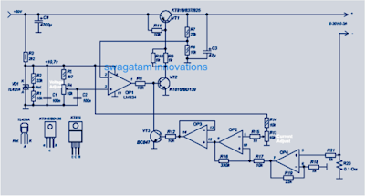
Referring to the above proposed universal power supply circuit diagram, the functional details can be understood with the help of the flowing points:
The IC LM324 forms the heart of the circuit and becomes responsible for all the involved complex processing.
Its a quad opamp IC meaning it has four opamps in one package, and all the 4 opamps (OP1----OP4) from this IC can be seen effectively employed for their respective functionalities.
The input supply which is derived either from a mains transformer or from a solar panel is suitably stepped down using a shunt zener network VD1 to provide a safe operating voltage for the IC LM324 and also for generating a stabilized reference for OP1 non-inverting input, via R5 and preset R4.
OP1 is basically configured as a comparator, wherein its pin3 is applied with a set reference, and its pin2 is connected with a potential divider across the output of the power supply for detecting the final voltage across the load.
Depending upon the setting of the R4 which can be a pot, the OP1 compares the level of the output voltage delivered by VT1 and trims it down to the specified level. Thus, the pot R4 becomes responsible for determining the effective output voltage and can be adjusted continuously for getting the desired voltage across the indicated output terminals of the circuit.
The above operation takes care of the variable voltage feature of the proposed universal power supply circuit. VT1 and VT2 must be appropriately selected as per the input voltage range for enabling the devices to perform correctly without getting damaged.
The variable current feature of the design is implemented through the remaining three opamps, that is collectively by the opamps OP2, OP3, and OP4.
OP4 is configured as a voltage sensor and amplifier, and it monitors the voltage developed across R20.
The sensed signal is fed to the input of OP2 which compares the level with a reference level set by the pot (or preset) R13.
Depending on the setting of R13, OP2 toggles OP3 continuously such that the output from OP3 switches off the driver stage VT1/VT2 whenever the output current tends to go above the fixed level (set by R13).
Therefore R13 here can be effectively used for setting up the maximum allowable current across the output for the connected load.
The resistor R20 may be appropriately dimensioned for calibrating the maximum allowable current for the load, which can be tweaked by R13 from 0 to maximum.
The above versatile features makes this universal power supply circuit extremely efficient, accurate and fail proof so that it can be used for most electronic application one can think of.
The design can be expected to be fully short circuit and overload protected, provided VT1 and VT2 are appropriately cooled by mounting them over adequate heatsinks.
The design of a simple opamp based power supply is not complex and utilizes ordinary parts such as IC LM324, a few BJTs and other associated passive components, yet it is too flexible and can be calibrated to any desired voltage and current range, right from 0 to 100V, or 0 to 100 amps.
I accidentally found this design from an online website and found it quite interesting, although I already have a similar design published in this site by the name zero drop solar charger circuit, the above shown circuit looks more meticulously designed and therefore is more accurate.
Referring to the above proposed universal power supply circuit diagram, the functional details can be understood with the help of the flowing points:
The IC LM324 forms the heart of the circuit and becomes responsible for all the involved complex processing.
Its a quad opamp IC meaning it has four opamps in one package, and all the 4 opamps (OP1----OP4) from this IC can be seen effectively employed for their respective functionalities.
The input supply which is derived either from a mains transformer or from a solar panel is suitably stepped down using a shunt zener network VD1 to provide a safe operating voltage for the IC LM324 and also for generating a stabilized reference for OP1 non-inverting input, via R5 and preset R4.
OP1 is basically configured as a comparator, wherein its pin3 is applied with a set reference, and its pin2 is connected with a potential divider across the output of the power supply for detecting the final voltage across the load.
Depending upon the setting of the R4 which can be a pot, the OP1 compares the level of the output voltage delivered by VT1 and trims it down to the specified level. Thus, the pot R4 becomes responsible for determining the effective output voltage and can be adjusted continuously for getting the desired voltage across the indicated output terminals of the circuit.
The above operation takes care of the variable voltage feature of the proposed universal power supply circuit. VT1 and VT2 must be appropriately selected as per the input voltage range for enabling the devices to perform correctly without getting damaged.
The variable current feature of the design is implemented through the remaining three opamps, that is collectively by the opamps OP2, OP3, and OP4.
OP4 is configured as a voltage sensor and amplifier, and it monitors the voltage developed across R20.
The sensed signal is fed to the input of OP2 which compares the level with a reference level set by the pot (or preset) R13.
Depending on the setting of R13, OP2 toggles OP3 continuously such that the output from OP3 switches off the driver stage VT1/VT2 whenever the output current tends to go above the fixed level (set by R13).
Therefore R13 here can be effectively used for setting up the maximum allowable current across the output for the connected load.
The resistor R20 may be appropriately dimensioned for calibrating the maximum allowable current for the load, which can be tweaked by R13 from 0 to maximum.
The above versatile features makes this universal power supply circuit extremely efficient, accurate and fail proof so that it can be used for most electronic application one can think of.
The design can be expected to be fully short circuit and overload protected, provided VT1 and VT2 are appropriately cooled by mounting them over adequate heatsinks.
Available link for download